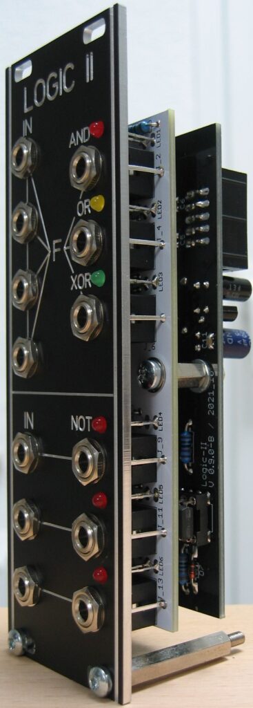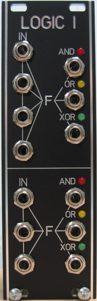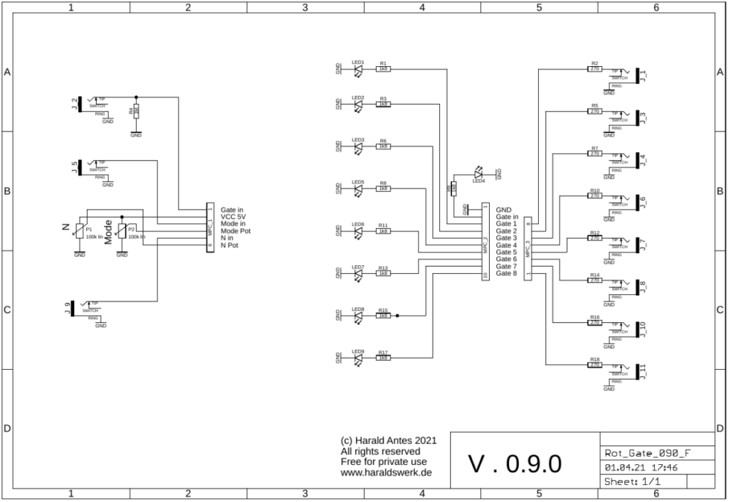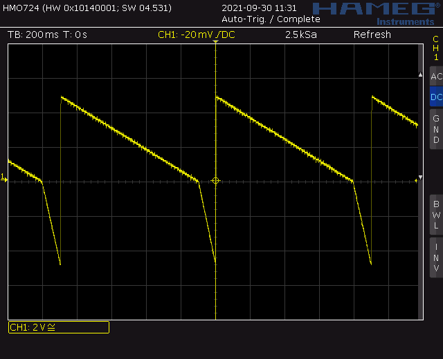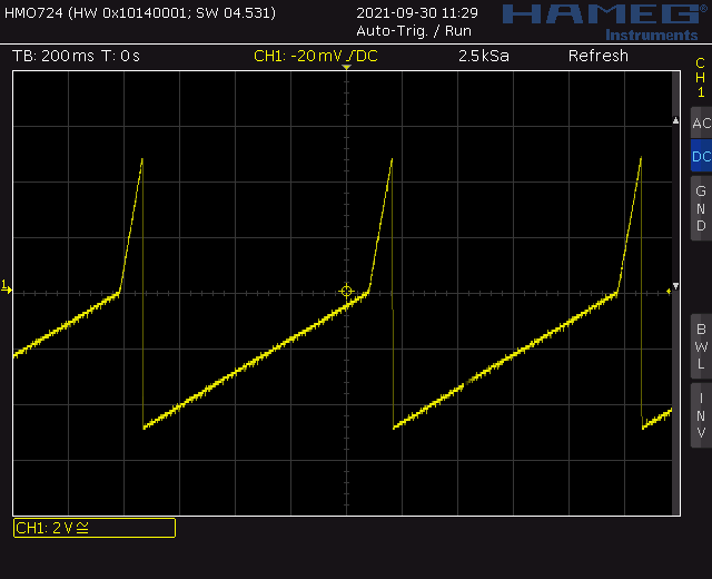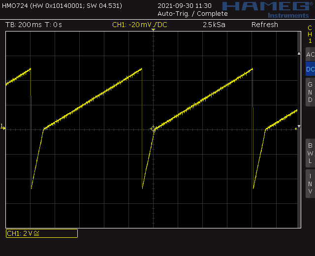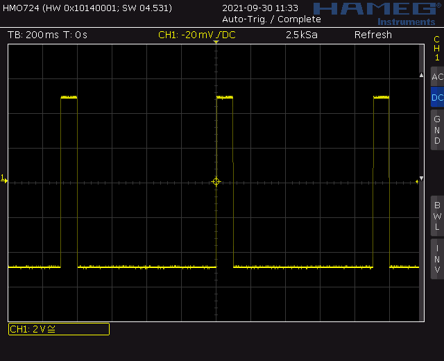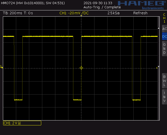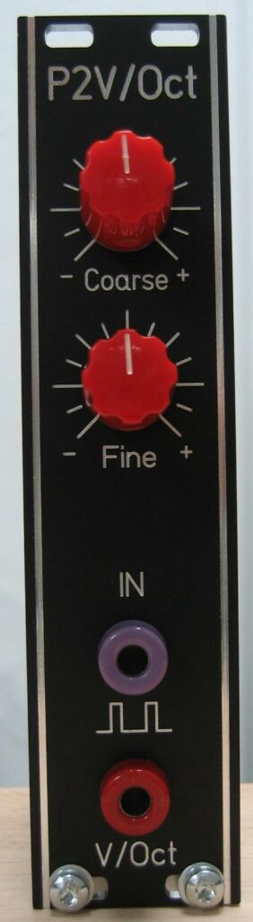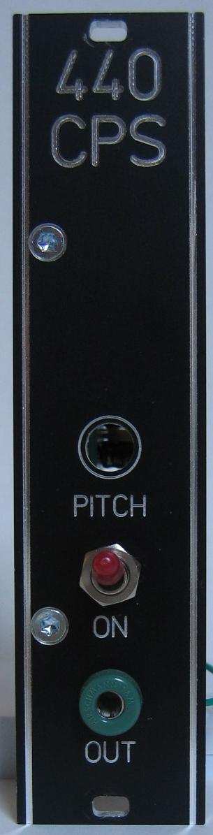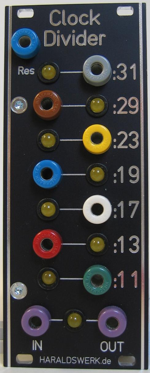
Clock Divider with prime numbers
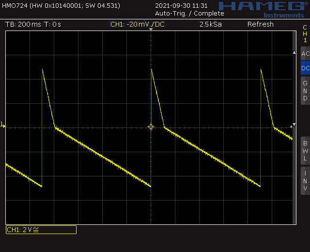
This clock divider divides the incoming clock signal down to the prime numbers /11, /13, /17, …. /31. The output is a 5V positive pulse. The length of the incoming pulse is kept. The trigger is on the rising edge of the incoming signal. The reset input can be used for syncing with other clocks. All outputs are buffered and brought out parallel with LED signaling the pulse.
Specs and features
• Regular input clock/square wave +5V
• Input signal divided by prime numbers
• Output +5V pulse with the length of the input signal (pulse)
• Runs with +15V/-15V or +12V/-12V (with minor changes)
The documentation for download can be found in my website.
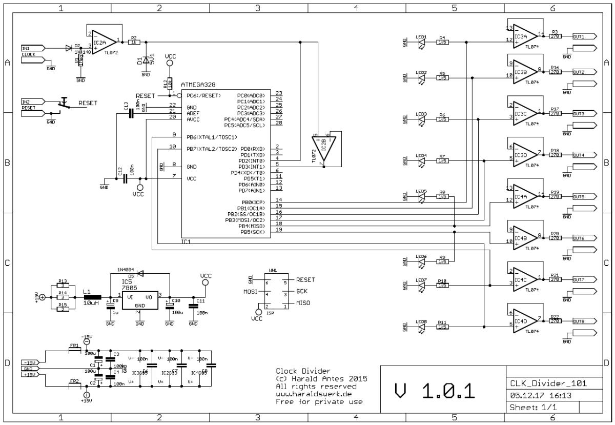
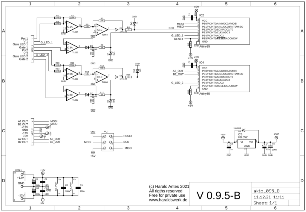
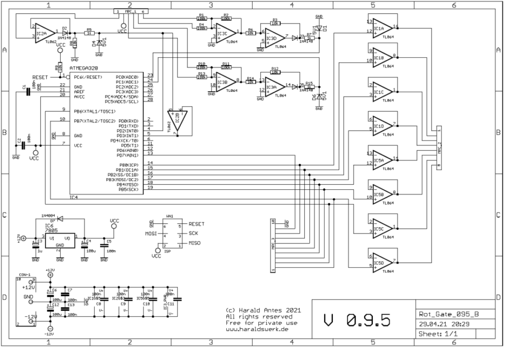
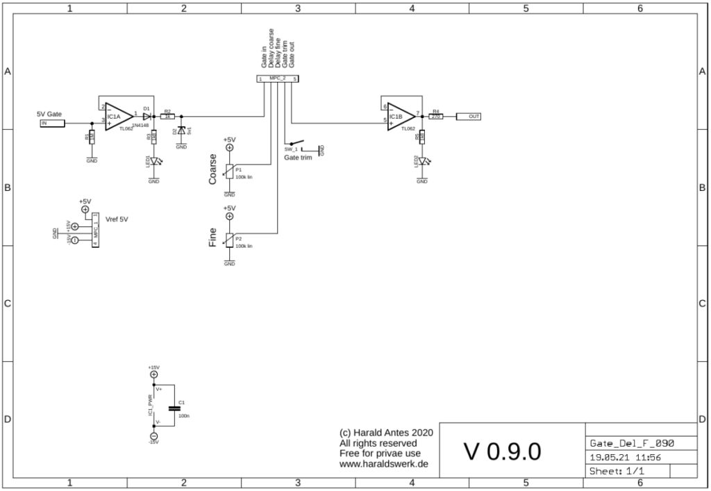
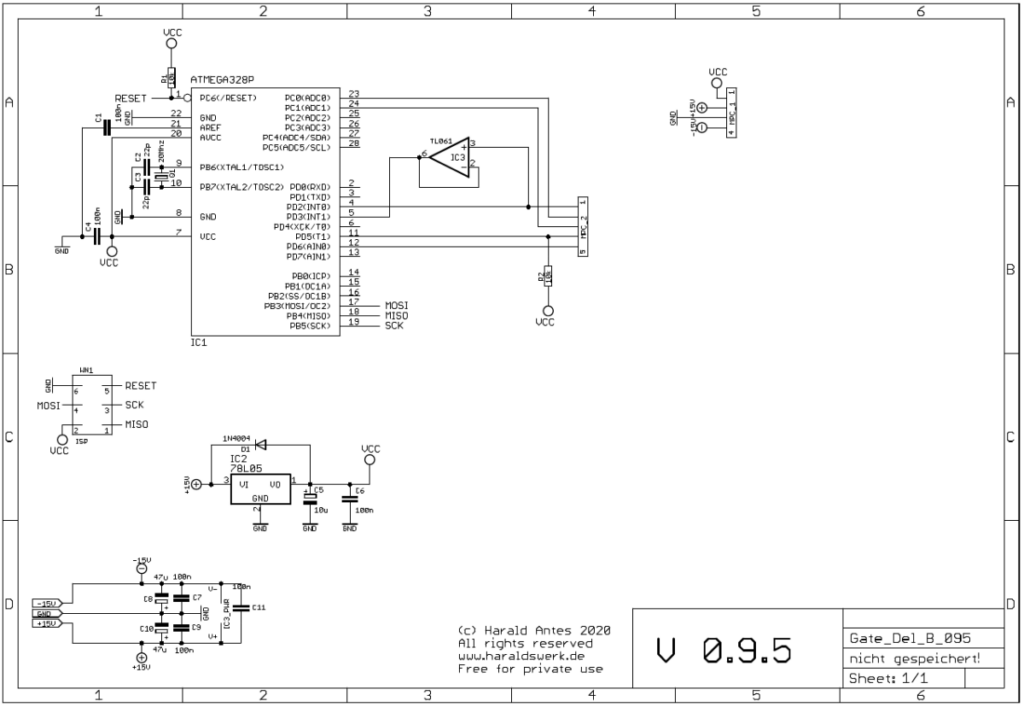
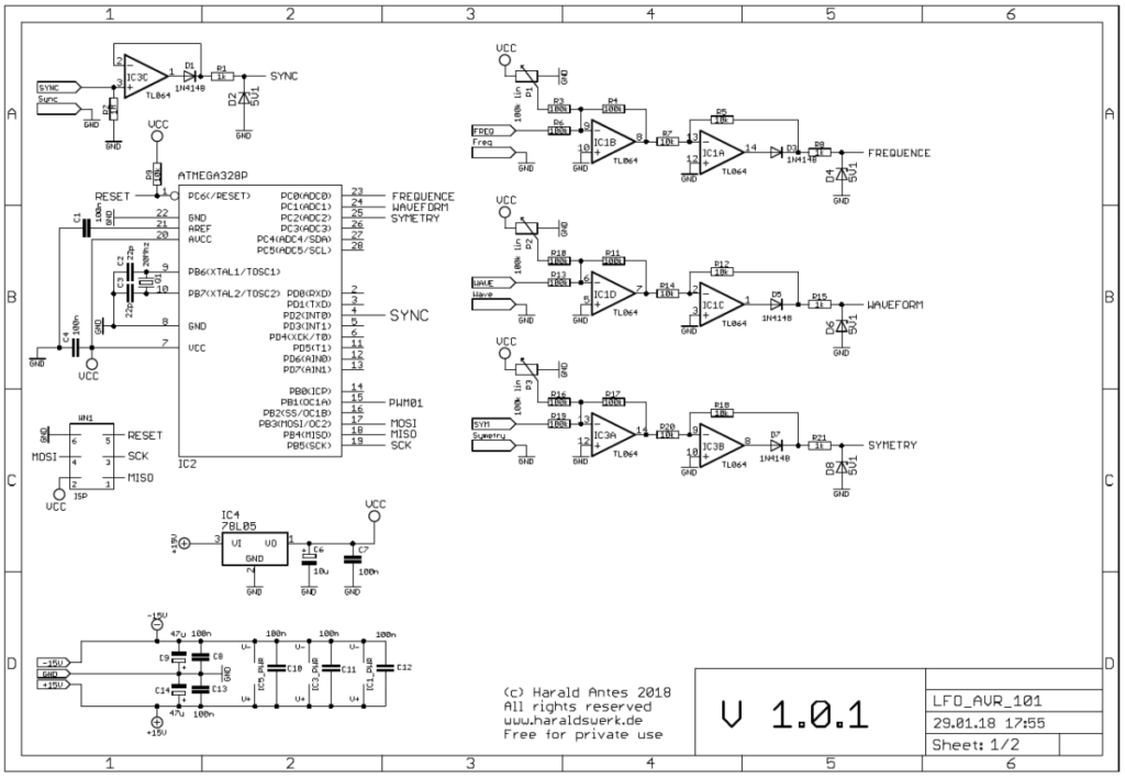
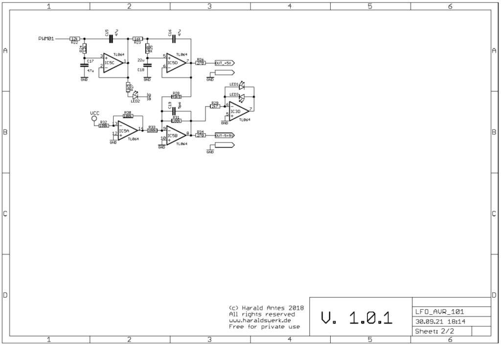
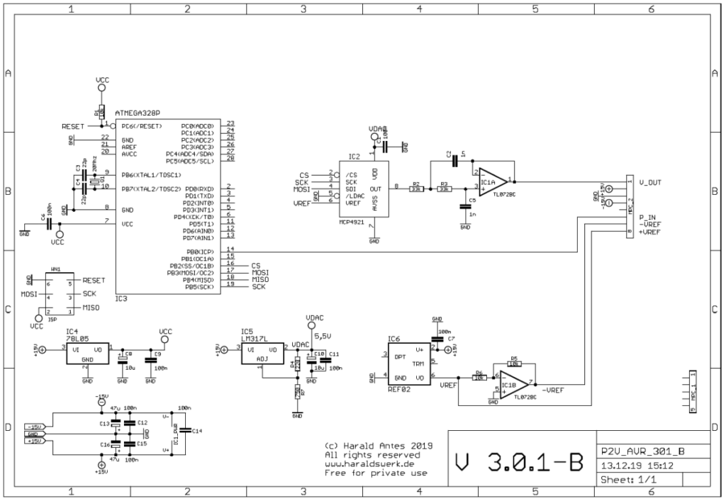
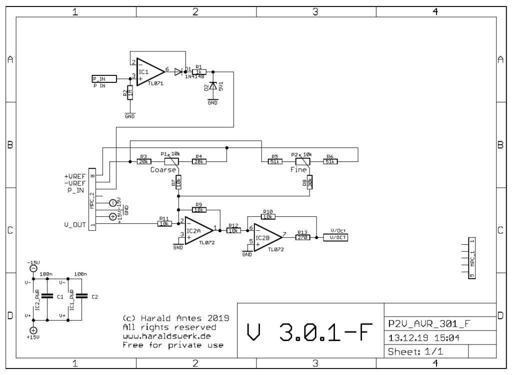
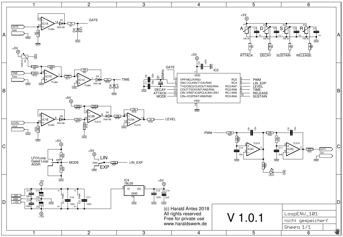
Clock Divider with prime numbers, schematic
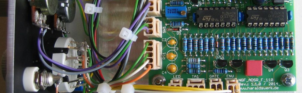
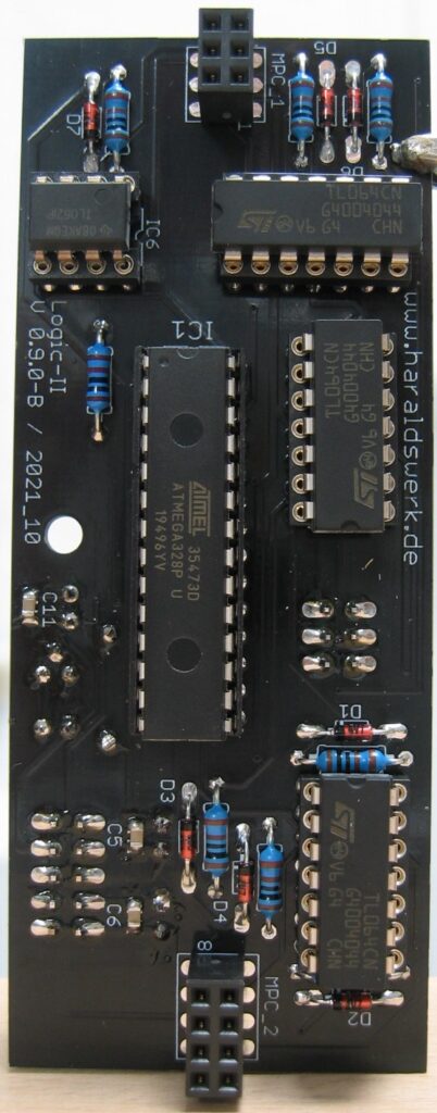
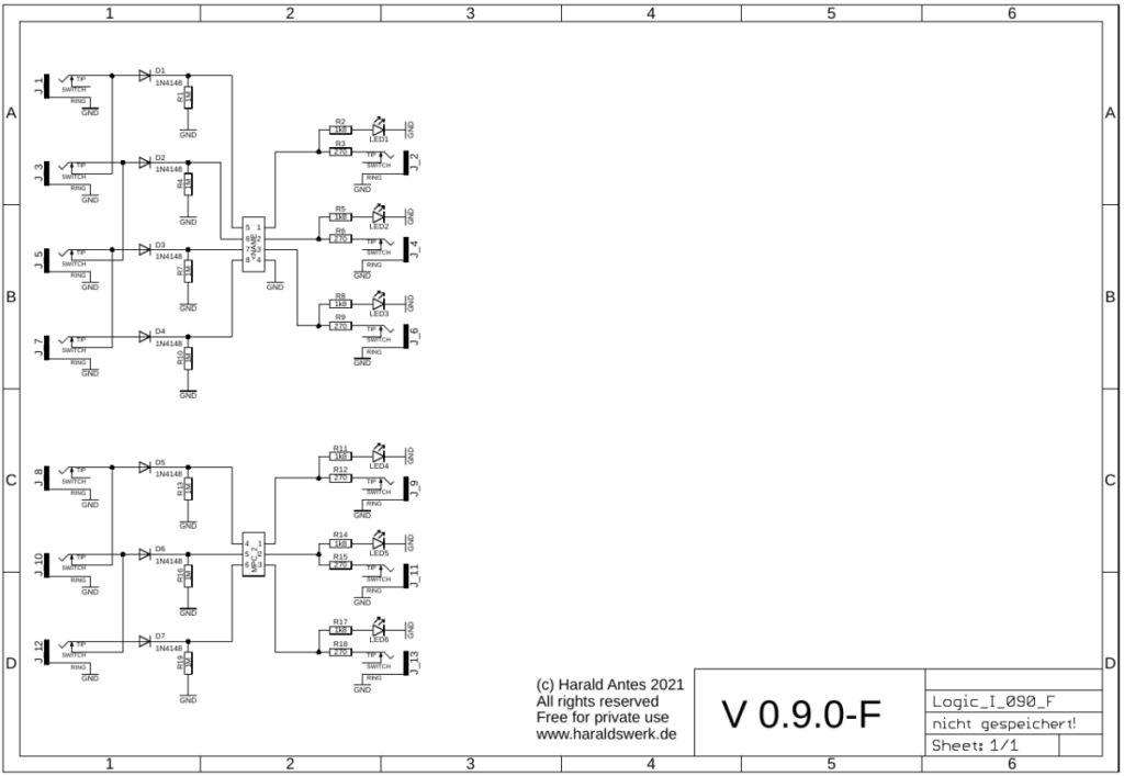
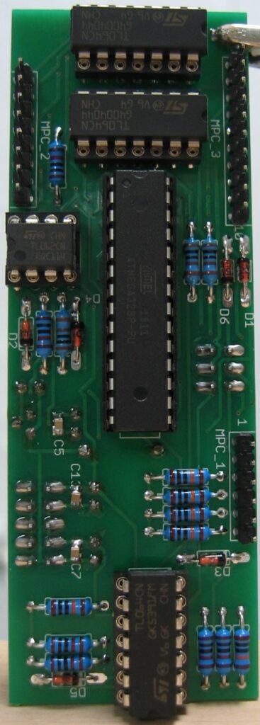
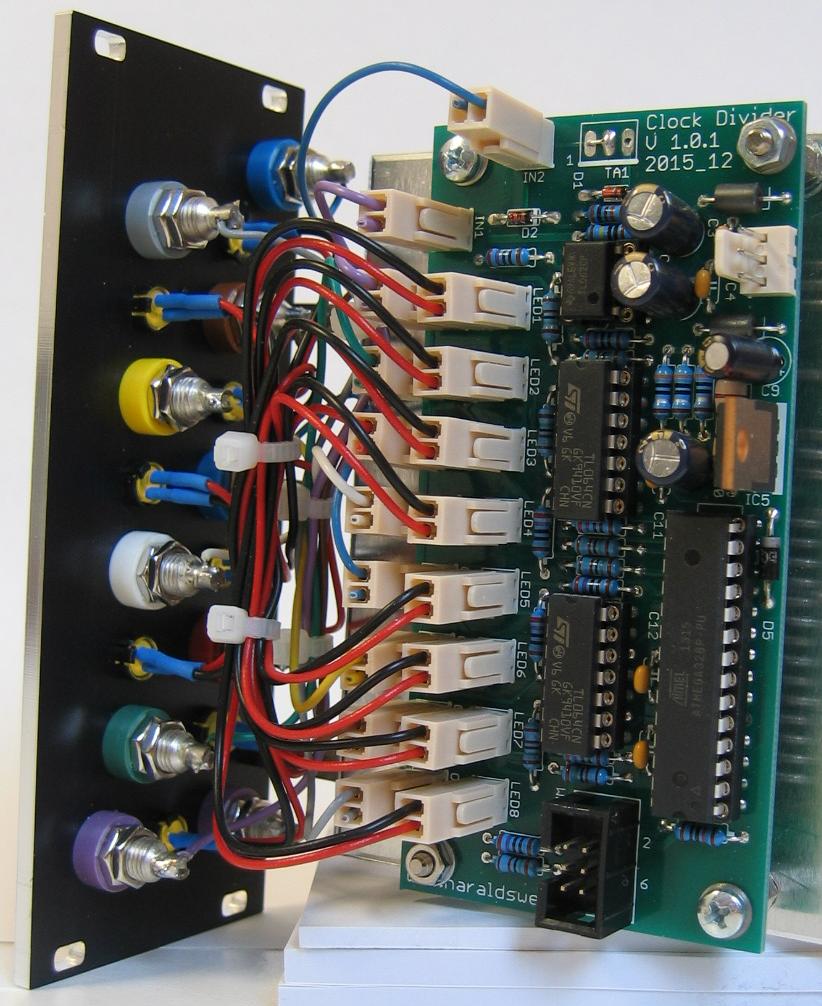
Most work is done by the microprocessor. The micro takes care of the input and output timing. All outputs are independently buffered. The clock is made visible with LED.
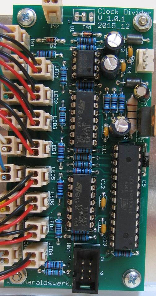
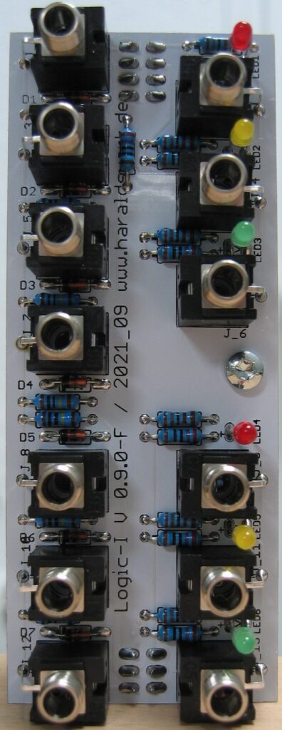
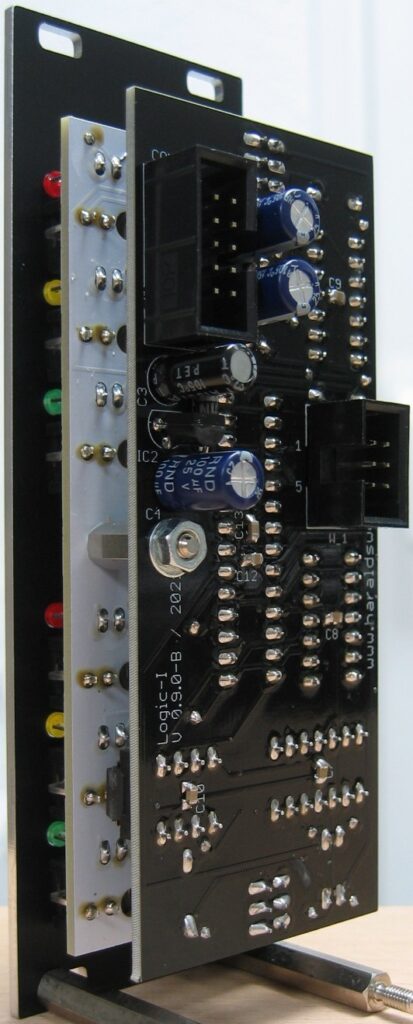
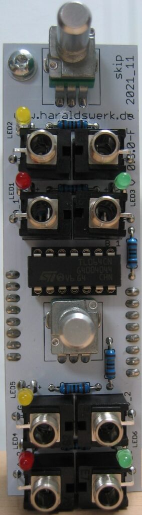
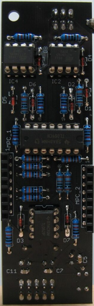
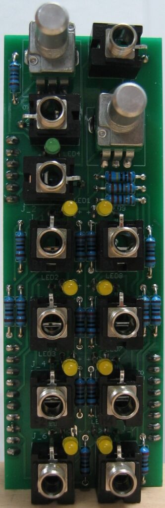
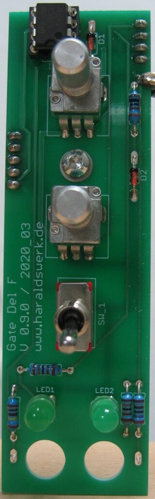
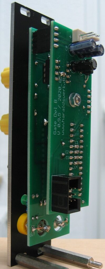
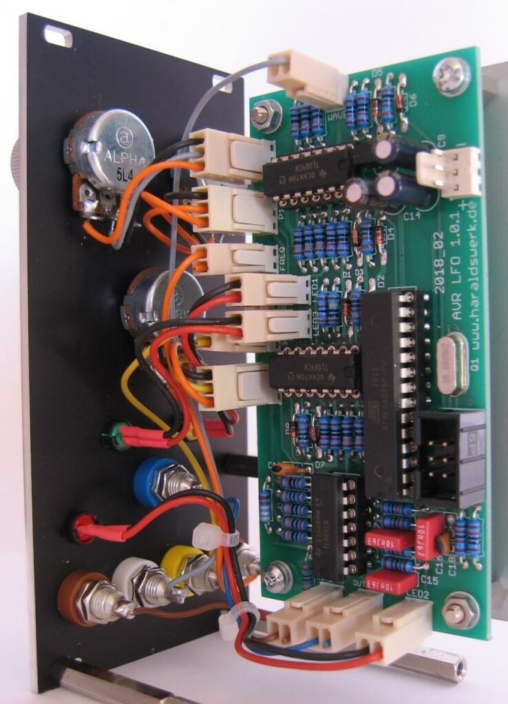
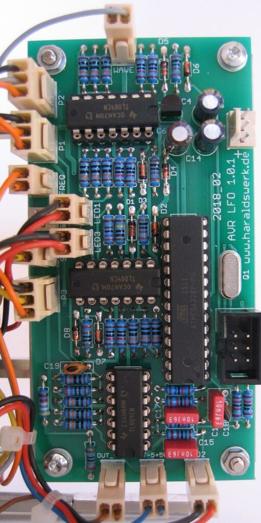
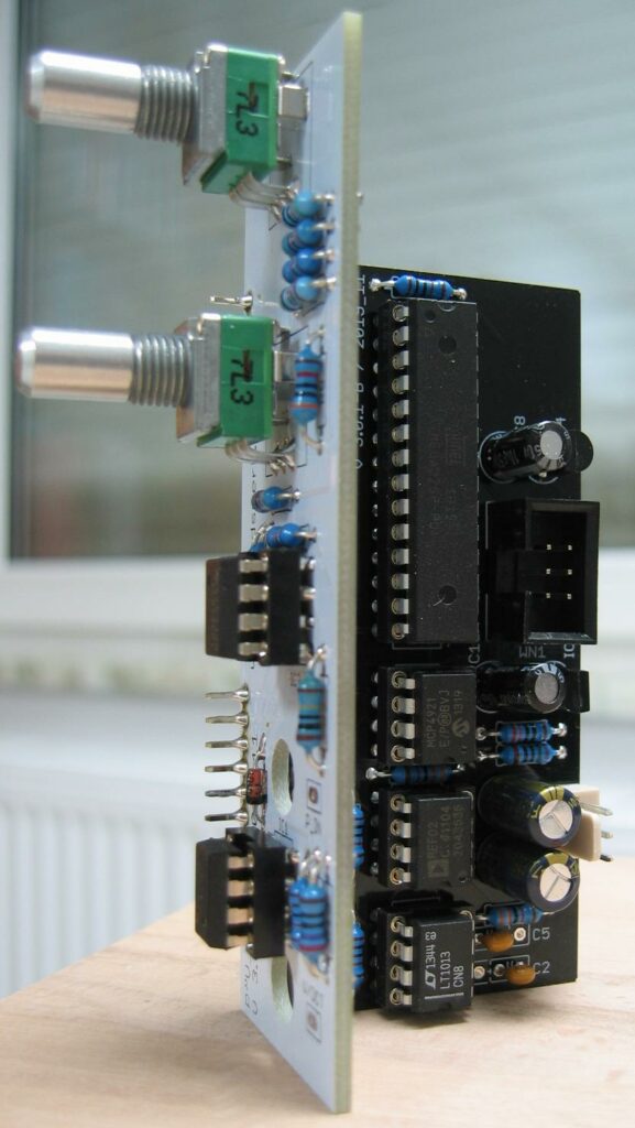
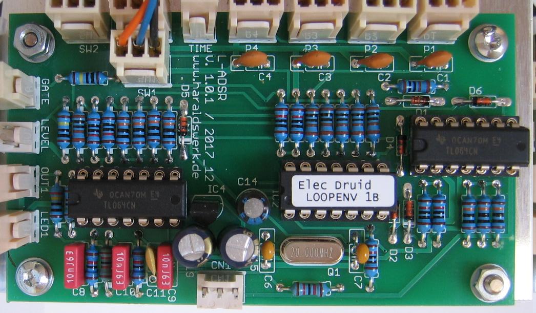
Clock Divider with prime numbers, populated PCB
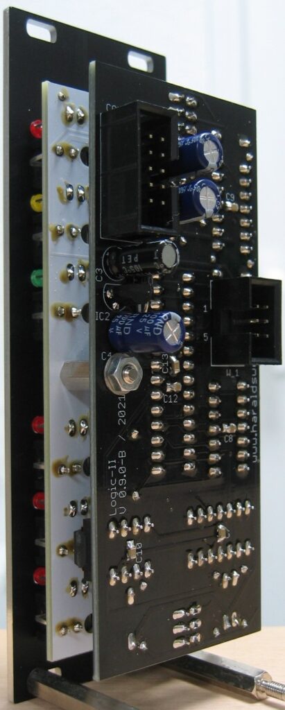
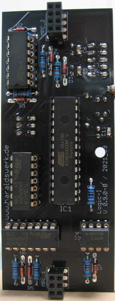
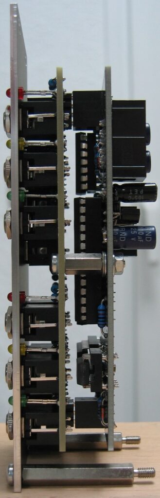
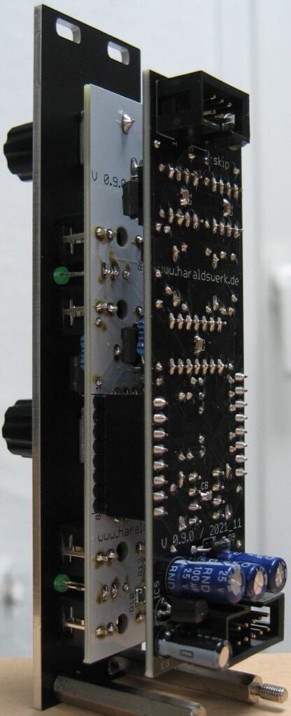
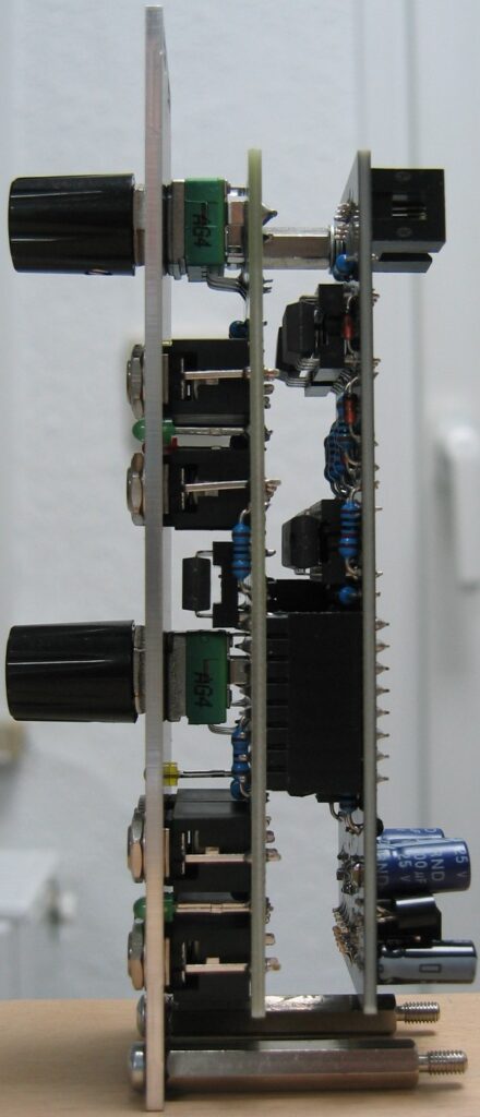
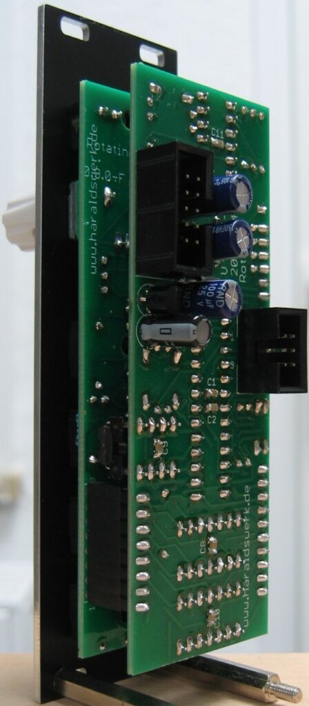
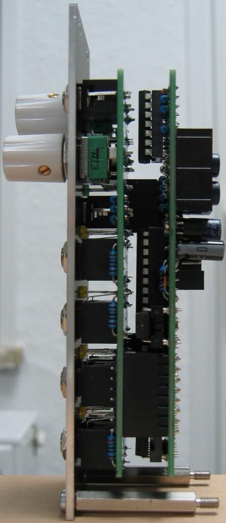
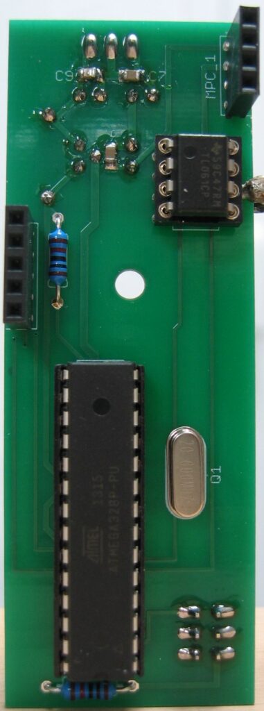
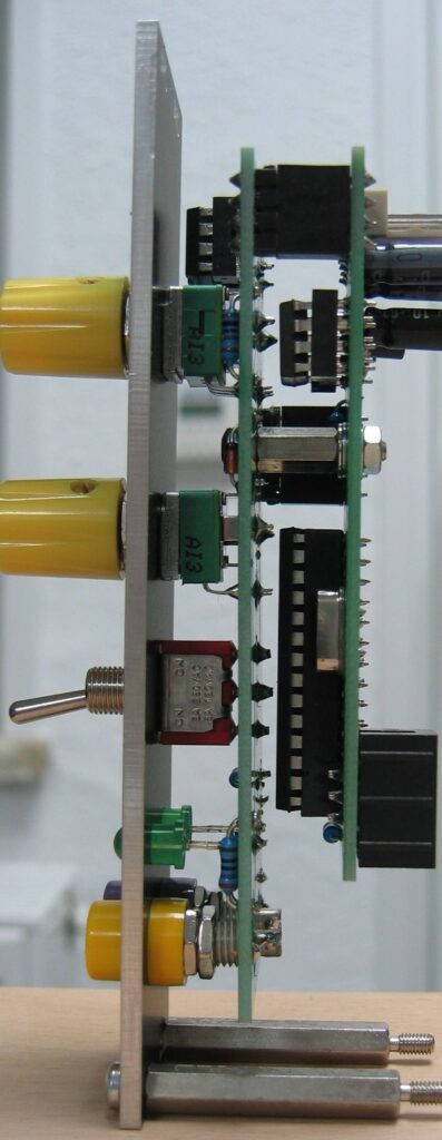
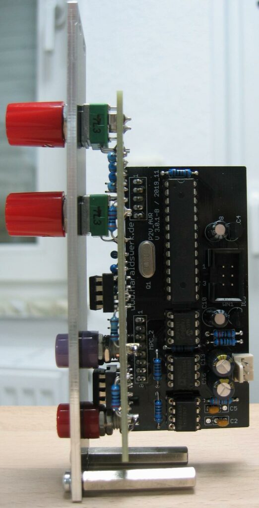
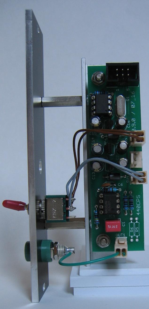
Clock Divider with prime numbers, rear view