Track (Sample) and Hold

Track (Sample) and Hold: Front view

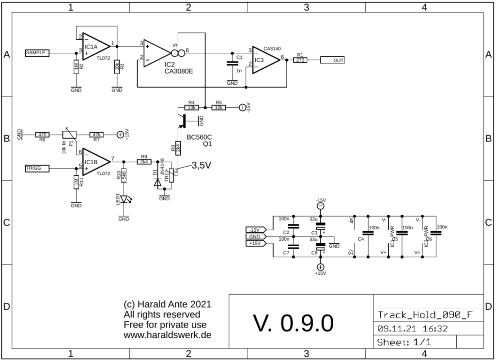
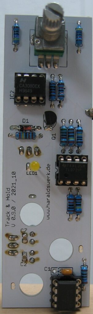
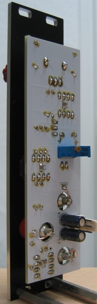
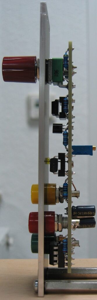
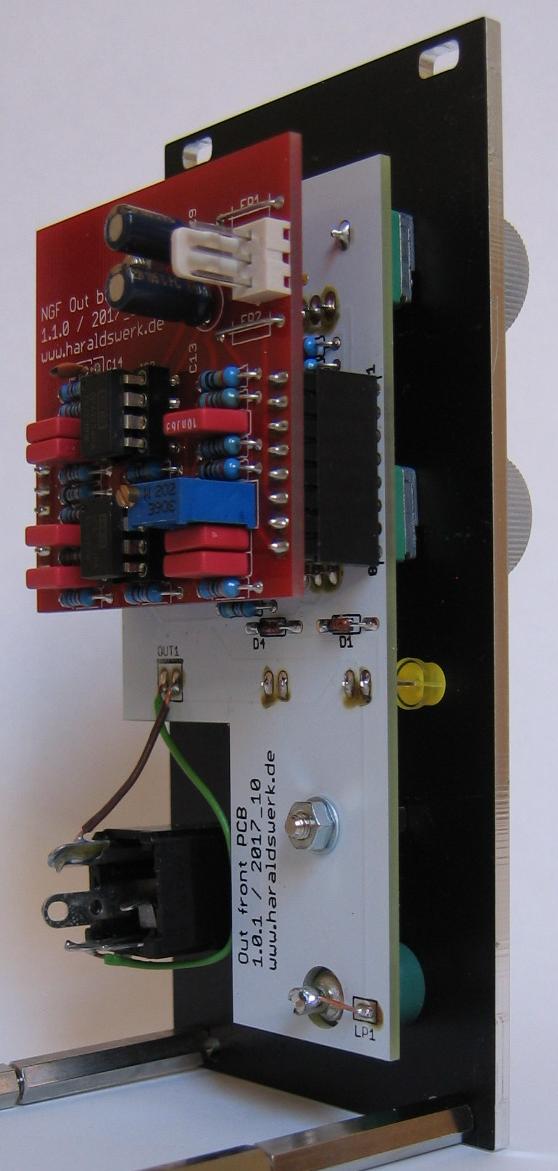
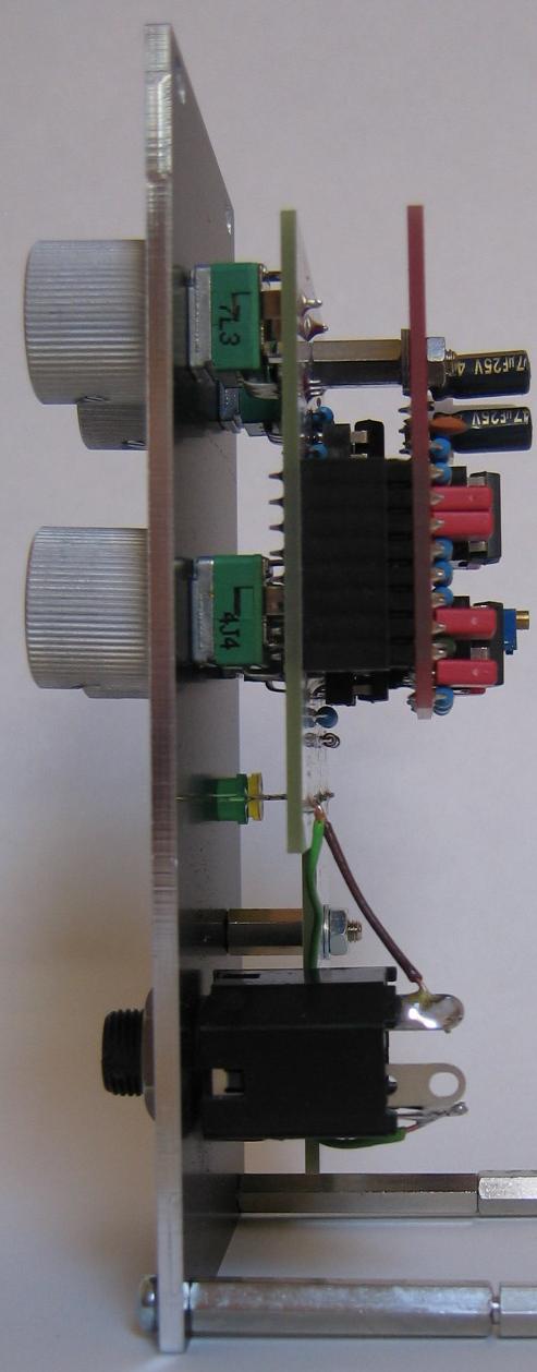
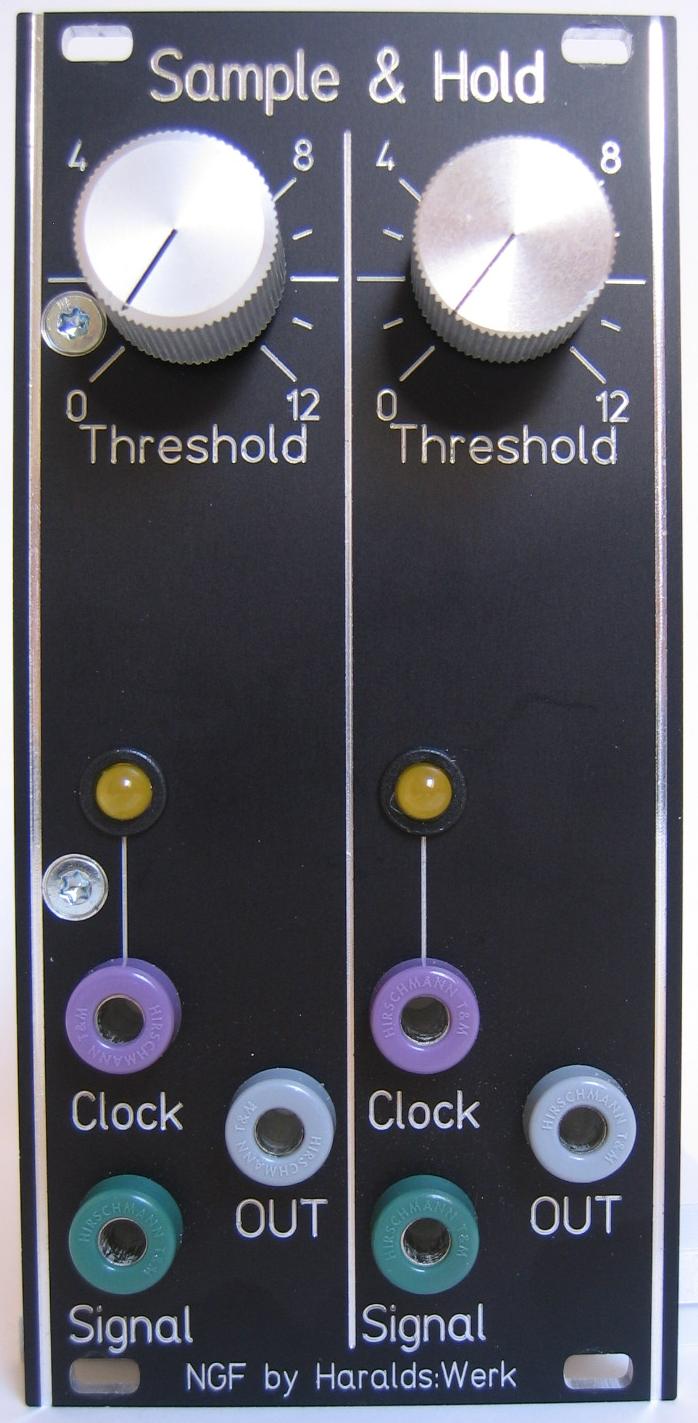
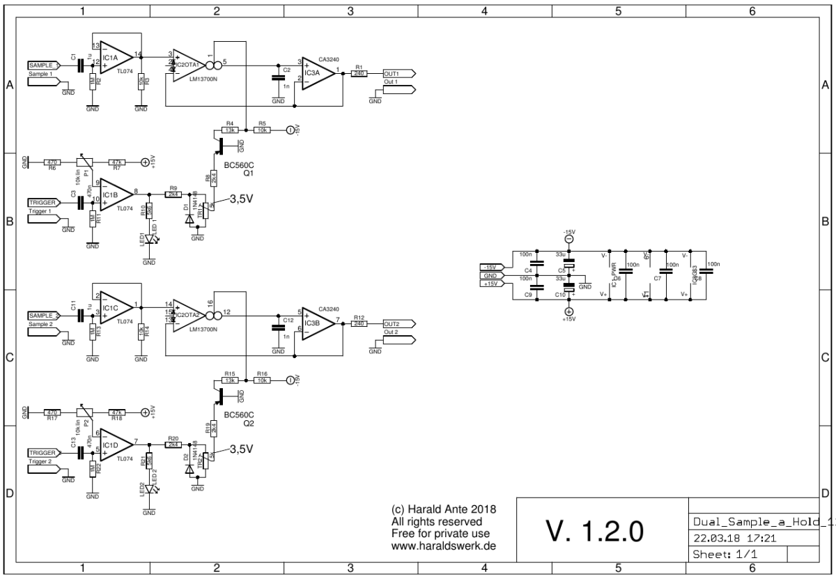
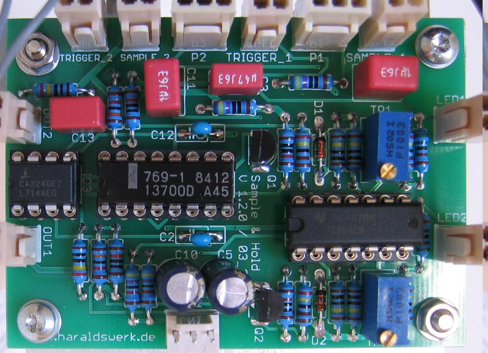
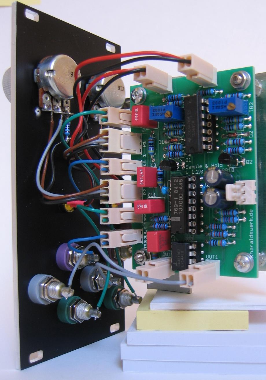
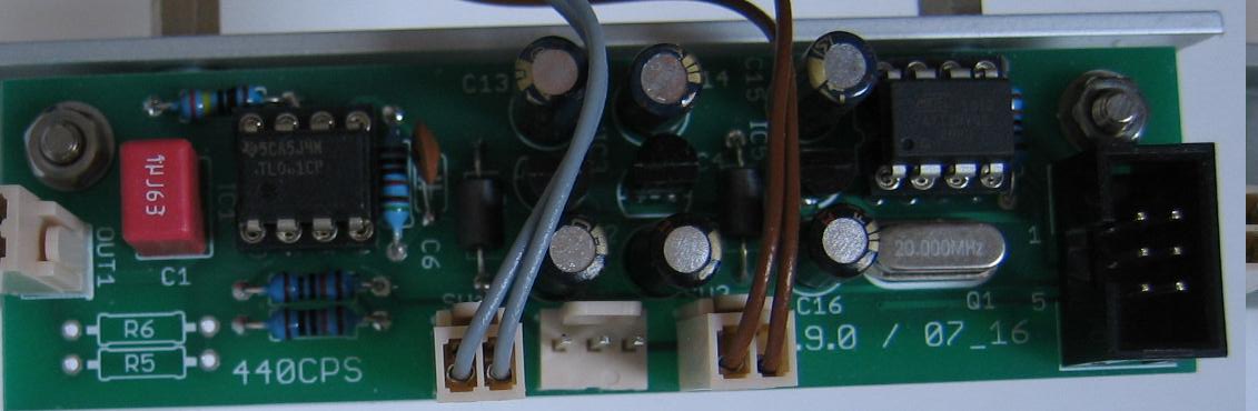
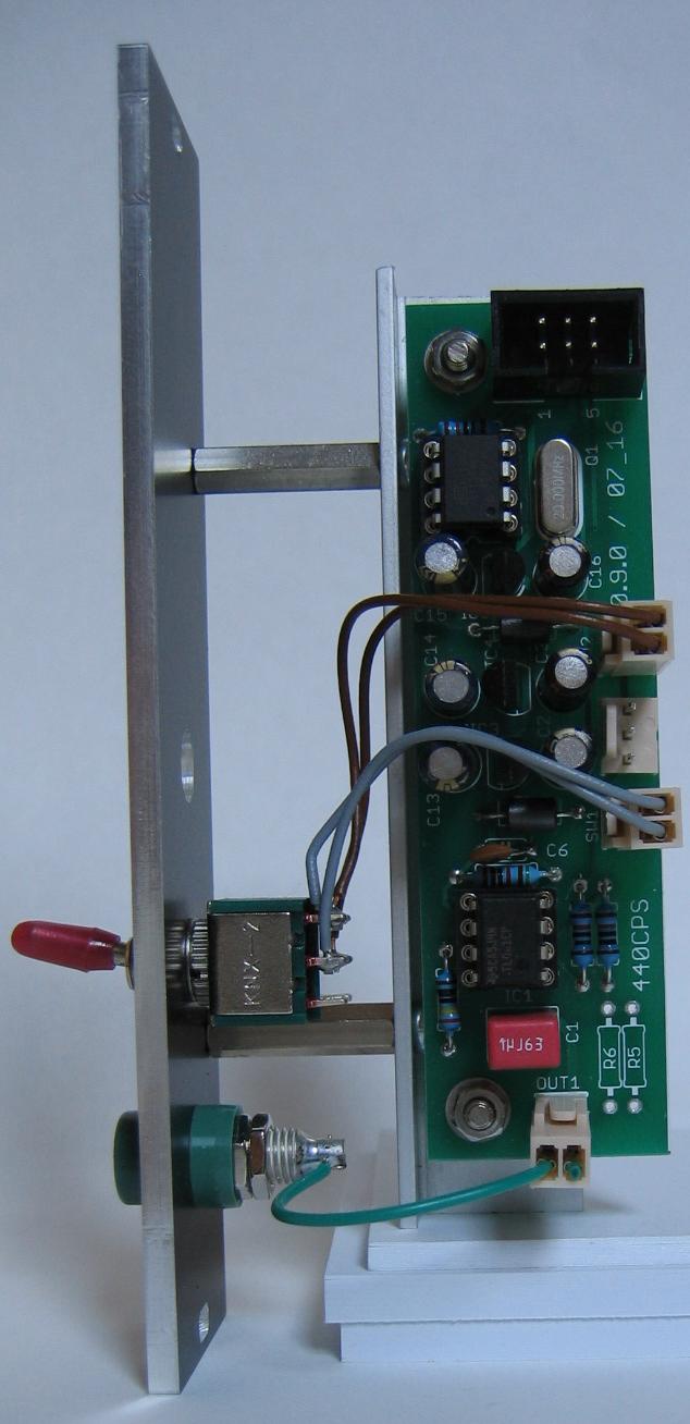
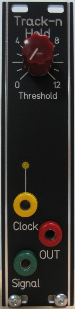
One more module for my Shakuhachi to Synths project. Not exclusively of course. This is a Track and Hold. Which is quite useful for other patches as well. In the Shakuhachi patch it is used to suppress an incomplete pitch to voltage conversion from the Pitch to voltage converter when the player stops blowing. The module tracks the incoming (control) voltage as long as the gate input is high. When the gate goes low the output voltage is kept. The module is DC coupled to track slowly moving voltages. For this one I have used some obsolete parts, which I had laying around. So, if you want to build it, make sure that you can get those parts. You can use it as Sample and Hold as well. Instead of a gate apply a trigger at the gate input.

Specs and features

  • Track or Sample and Hold
  • DC coupled
  • Gate input with LED
  • Signal input
  • Signal output
  • Threshold
  • Runs on +/-12V and +/-15V
  • Power consumption below 20mA each rail

The documentation and the Gerber files for download can be found in my website.

Track (Sample) and Hold: Schematic
Track (Sample) and Hold: Populated PCB
Track (Sample) and Hold: Back view
Track (Sample) and Hold: Side view

Output Module

Output Module: Front view

Output Module: Front view

This is my replacement of the original Elektor Formant COM module. I discarded the original circuitry because of the TL085 used with his unusual pinout and the availability of dedicated audio operational amplifiers. I used a more effective filter implementation for tone control. The tone control is derived from “Small Signal Audio Design” by Douglas Self Chapter 15. A optional level indicator makes it easier to find the right volume level for best SNR. The maximum output volume is adjustable to protect your PA. You can connect the output directly to active monitors.

Specs and features
• Bass, middle, treble tone control
• Adjustable maximum output volume
• Optional volume indicator
• Direct connection to active monitors
• Runs on +/-15V and +/-12V (with minor resistor changes)

The documentation for download can be found in my website.

Output Module: Schematic front PCB

Output Module: Schematic front PCB

Output Module: Schematic back PCB

Output Module: Schematic back PCB

A description can be found in “Small Signal Audio Design” by Douglas Self Chapter 15

Output Module: Stuffed PCB back view

Output Module: Stuffed PCB back view

Output Module: Stuffed PCB side view

Output Module: Stuffed PCB side view

Output Module: Side view

Output Module: Side view

NGF Project: Dual Sample and Hold

Dual Sample and Hold: front view

Dual Sample and Hold: front view

Storing analog signals is a often used function in analog synthesizers. This sample and hold implementation follows closely the original Elektor Formant version of Book 2 “Formant Erweiterungen” p84ff. It is build for my Next Generation Formant project. Because I use the LM13700 here as replacement for the CA3080 I have build a dual sample and hold version. The PCB size is reduced from 100x160mm for a single version to 50x70mm for the dual version.

Specs and features
• Dual sample and hold
• 10Vpp input and output
• Runs on +/-15V and +/-12V
• Power consumption below 25mA each rail

The documentation for download can be found in my website.

Dual Sample and Hold: schematic

Dual Sample and Hold: schematic

This implementation follows closely the original Elektor Formant implementation. Refer to the original documentation if needed. You can find it on the net. My changes are the input buffers, using the LM13700 instead of the CA3080 and the adaption to my 10Vpp signal level.

Dual Sample and Hold: populated PCB

Dual Sample and Hold: populated PCB

Dual Sample and Hold: back view

Dual Sample and Hold: back view

NGF Project: 440CPS

NGF-E Project: 440CPS front view

NGF-E Project: 440CPS front view

Not much to say. A 440CPS module. Quite useful for tuning in a bigger system. OK, one more sentence. It is the replacement for the 440CPS module from the Elektor Formant in my Next Generation Formant project Project.

Specs and features
• On/Off Switch to keep the 440Hz out of the system when not needed
• Runs on +/-15V and +/-12V
• Power consumption below 25mA +rail / 5mA -rail

The documentation for download can be found in my website.

NGF-E Project: 440CPS schematic

NGF-E Project: 440CPS schematic

Everything is done in software. Output is a 440Hz Square wave. That’s it.

NGF-E Project: 440CPS populated PCB

NGF-E Project: 440CPS populated PCB

NGF-E Project: 440CPS back view

NGF-E Project: 440CPS back view

NGF-Project: Elektor Wave Processor

NGF Project: Elektor Wave Processor

NGF Project: Elektor Wave Processor

A small but very versatile module. It is derived from the original Elektor Formant book “Formant Erweiterungen” p87 ff. Some resistor values are changed to handle the 10Vpp signal level of my system. You can shape the input signal in many ways. You can clip the signal. You can fold the signal. You can emphasize the third harmonic. You can unsymmetrical emphasize the clipped and unclipped signal. You can reverse the input signal. The clipping level is voltage controlled.

Specs and features

• Clipping the signal
• Folding the signal
• Emphasize the third harmonic
• Unsymmetrical emphasize the clipped and unclipped signal
• Clipping level voltage controlled
• 10Vpp input and output
• Runs on +/-15V and +/-12V

The documentation for download can be found in my website.

NGF Project: Elektor Wave Processor, schematic

NGF Project: Elektor Wave Processor, schematic

This implementation follows closely the original Elektor Formant implementation. Refer to the original documentation if needed. You can find it on the net. My changes are the adaption to my 10Vpp system signal level.

NGF Project: Elektor Wave Processor, populated PCB

NGF Project: Elektor Wave Processor, populated PCB

NGF Project: Elektor Wave Processor, rear view

NGF Project: Elektor Wave Processor, rear view

NGF Project: Dual Ringmodulator

NGF Project: Dual Ringmodulator front view

NGF Project: Dual Ringmodulator front view

I was a bit hesitant doing this module because it uses the now obsolete LM1496 balanced modulator-demodulator. But you can still source them and I have some in my stock. So I decided to make a PCB and module for my Next Generation Formant project. I started with the original Elektor Formant schematic published in “Formant Erweiterungen” p35ff. I left out the microphone and envelope follower part because I already have such modules. I have added input buffers and raised the signal level to my 10Vpp used throughout my system. I was able to put two ringmodulator on a 50x100mm PCB.

Specs and features
• Dual ringmodulator
• 10Vpp input and output
• Runs on +/-15V and +/-12V

The documentation for download can be found in my website.

NGF Project: Dual Ringmodulator schematic

NGF Project: Dual Ringmodulator schematic

This implementation follows closely the original Elektor Formant implementation. Refer to the original documentation if needed. You can find it on the net. My changes are the input buffers and the adaption to my 10Vpp signal level.

NGF Project: Dual Ringmodulator populated PCB

NGF Project: Dual Ringmodulator populated PCB

NGF Project: Dual Ringmodulator back view

NGF Project: Dual Ringmodulator back view

NGF-E Project: Mix Out (COM)

NGF-E Project: Mix Out (COM) stuffed PCB

NGF-E Project: Mix Out (COM) stuffed PCB

This is my replacement of the original Elektor Formant COM module used in my Next Generation Formant project. I discarded the original circuitry because of the TL085 used with his unusual pinout and the availability of dedicated audio operational amplifiers. I used a more effective filter implementation for tone control. A mixer front end with four external inputs is added to make patching easier. A optional level indicator makes it easier to find the right volume level for best SNR. The maximum output volume is adjustable to protect your PA

The documentation for download can be found in my website.

NGF-E Project: Mix Out (COM) schematic

NGF-E Project: Mix Out (COM) schematic

Nothing special in this schematic. The tone control is a Baxandall type.
Calibration procedure and more information on my website.

NGF-E Project: Mix Out (COM) front view

NGF-E Project: Mix Out (COM) front view

NGF-E Project: Mix Out (COM) back view

NGF-E Project: Mix Out (COM) back view

NGF-E Project: ADSR

NGF-E Project: ADSR stuffed PCB

NGF-E Project: ADSR stuffed PCB

This is my take on the ADSR. Because this one is for my Next Generation Formant project i started with the original Elektor Formant ADSR schematic and added my changes to the design. All parts are updated to today (2017/09) available parts. The connections are the same as in the original to keep the possibility for internal wiring. If you don’t need those features just leave them out. This PCB provides all functions as in the original Elektor Formant ADSR. I have made a few changes to fix some shortcomings of the original. A triple range switch was added for finer adjustment of the ADSR CV-output signal. The attack rise time is shorter now as in the original. The gate input is buffered. The fixes a fault in the original when working with analog sequencers. The output voltage is slightly raised to reach really 5V. Due to the design of the original Elektor Formant ADSR the output of the original ADSR keeps a residual voltage of about 0,5V. I have put an adjustable compensation in my design to correct this and keep the original behavior if needed as well.

The documentation for download can be found in my website.

NGF-E Project: ADSR schematic

NGF-E Project: ADSR schematic

This is a close clone of the Elektor Formant ADSR. Here i only describe the changes i have made. The description of the other parts of the circuitry can be found in the original Elektor Formant documentation. The gate signal input resistance is raised from 33kOhm to 1megOhm with the input buffer IC1A. This protects against double triggering with the falling edge of the gate signal when using sequencers. R12 is used to fix the input to a defined potential when no signal is attached to the input. R33 and R36 in combination with a push button give you the single shot feature. C1 was lowered to 6n8 from 10nF. In combination with C2 and the raised charging voltage through IC1B/R9 this makes for faster attack time. The load capacitor of 10u was replaced with three selectable capacitors of 2,2uF 4,7uF and 10uF. This make for a finer adjustment of the response times of the ADSR. The voltage divider R24/R25 was adjusted to ensure that the output level of 5V is reached when the offset option with TR2 is used. If this feature is not used R25 should be lowered to 5k1. Construction conditioned the output at IC1D only reaches a minimal voltage of about 0,5V. To compensate for this i added IC2C. With TR2 you can trim the output down to zero volts. If the ADSR is not used the output voltage is now at -0,5V. If you don’t want to use this feature just turn TR2 to ground and you will have the original behavior of the original Elektor Formant ADSR. The current consumption was lowered with using the TL064 and a low current led.
Calibration procedure and more information on my website.

NGF-E Project: ADSR faceplate

NGF-E Project: ADSR faceplate

NGF-E Project: ADSR back

NGF-E Project: ADSR back

NGF-E Project: VCA

NGF-E Project: VCA stuffed PCB

NGF-E Project: VCA stuffed PCB

This is my take on the VCA. Because this one is for my Next Generation Formant project i started with the original Elektor Formant VCA schematic and added my changes to the design. All parts are updated to today (2017/08) available parts. The connections are the same as in the original to keep the possibility for internal wiring. If you don’t need those features just leave them out. This PCB provides all functions as in the original Elektor Formant VCA. The CA3080 are replaced with LM13700. The signal level is raised to 10Vpp for a better signal to noise ratio. The added volume indicator us useful for finding the appropriate signal level. The volume indicator is optional. You can leave it out with no problems for the other functions.

The documentation for download can be found in my website.

NGF-E Project: VCA schematic

NGF-E Project: VCA schematic

This is a close clone of the Elektor Formant VCA. It consists off two OTA’s in serial configuration. The first OTA provides the log response and the second one the linear response. IC2A sums up the external and internal audio signal. The circuitry around IC1A provides the log converter, IC1B the linear current source for the second OTA.
Calibration procedure and more information on my website.

NGF-E Project: VCA front view

NGF-E Project: VCA front view

NGF-E Project: VCA back view

NGF-E Project: VCA back view

NGF-E Project: LFO

NGF-E Project: LFO PCB

NGF-E Project: LFO PCB

Here is the LFO module for my NGF-E project. It provides triangle, ramp up, ramp down and square wave output (-5V to +5V) This design follows closely the original from the Elektor Formant.

The documenatation for download can be found in my website.

NGF-E Project: LFO schematic

NGF-E Project: LFO schematic

The oscillator consists of an integrator IC1A and an OpAmp Schmitt-Trigger IC1B. The triangle wave of the oscillator arises through the feedback of the trigger output to the input of the integrator. At the integrator output IC1A arises a triangle with the amplitude of the hysteresis of the Schmitt-Trigger. The input voltage of the integrator sets the rise and fall time of the voltage output. The square wave output is buffered with IC1C. The circuitry around IC1D provides the saw output. IC3C inverts the saw.

NGF-E Project: LFO faceplate

NGF-E Project: LFO faceplate