Sims style VCA for Eurorack

Sims style VCA: Front view

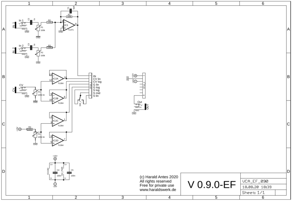
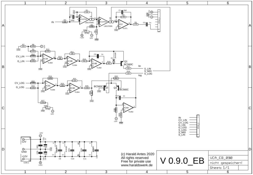
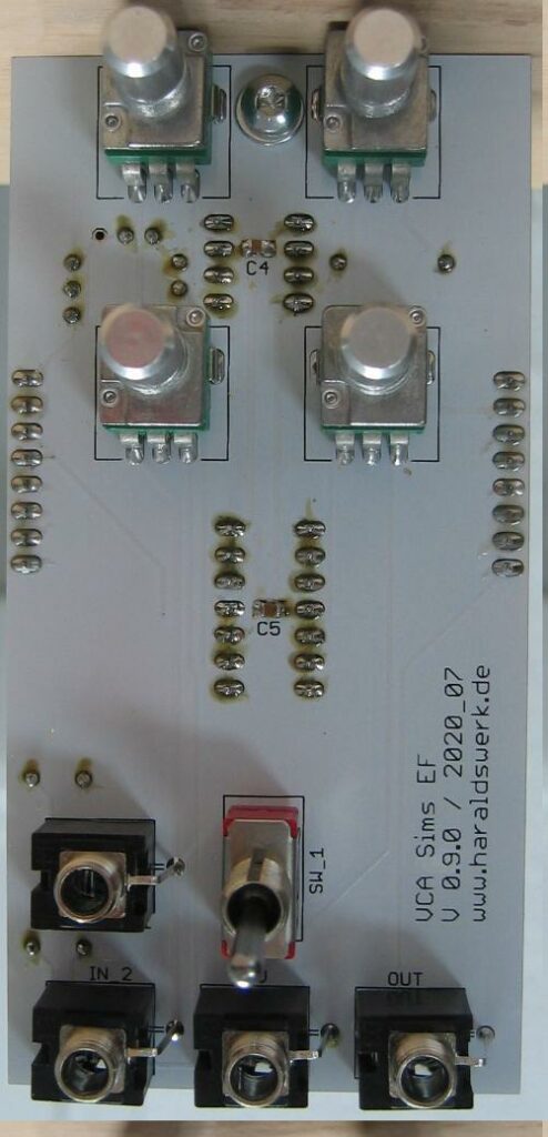
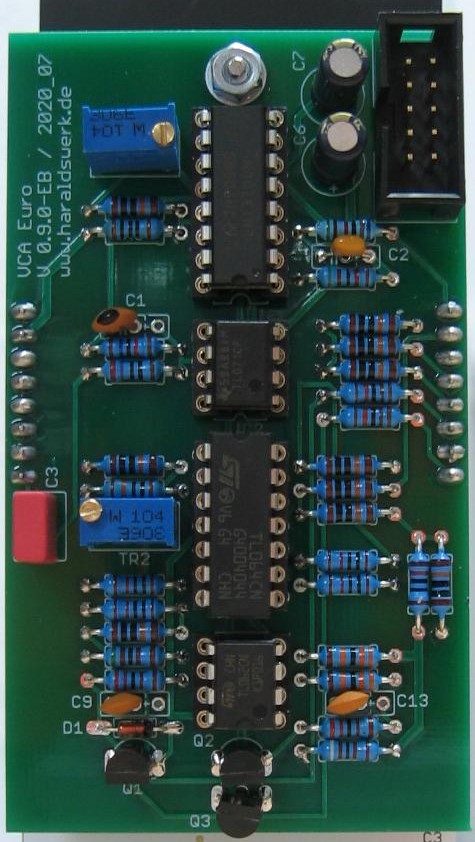
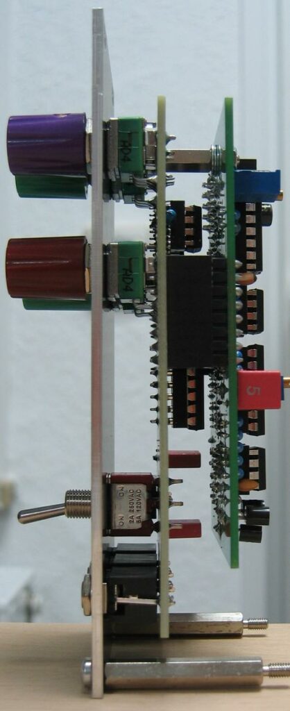
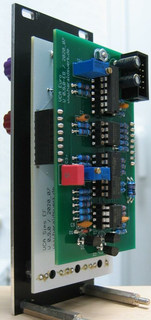
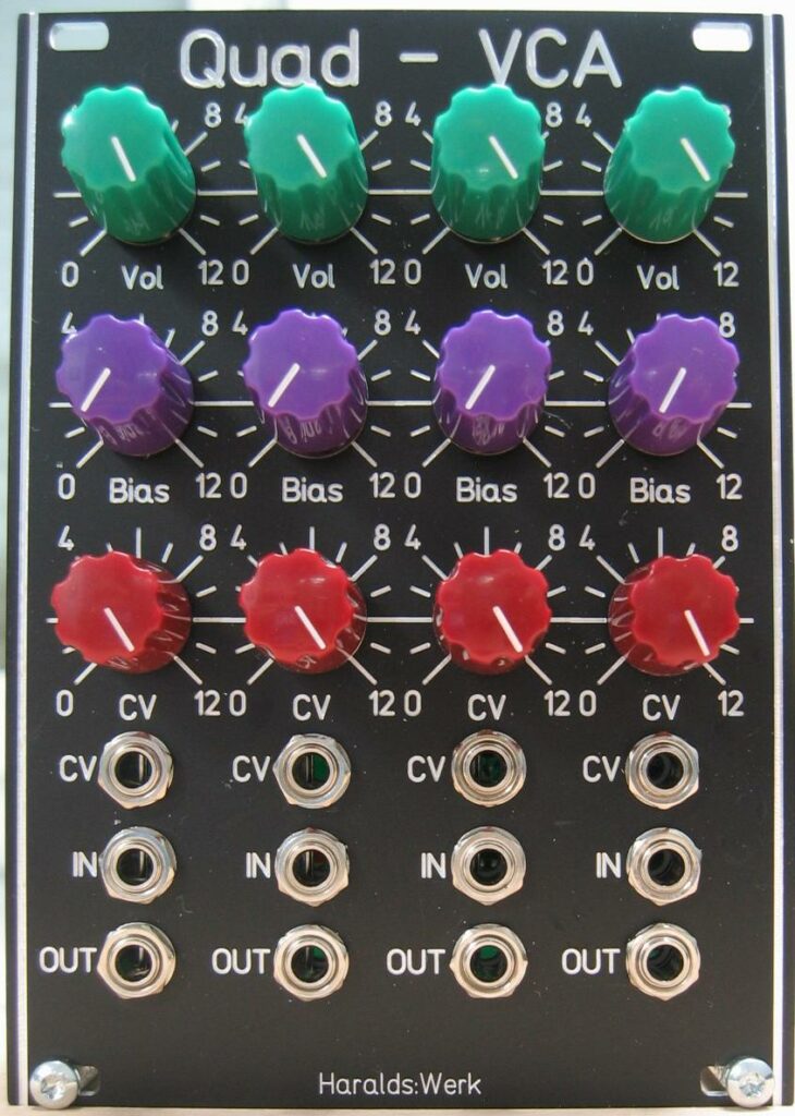
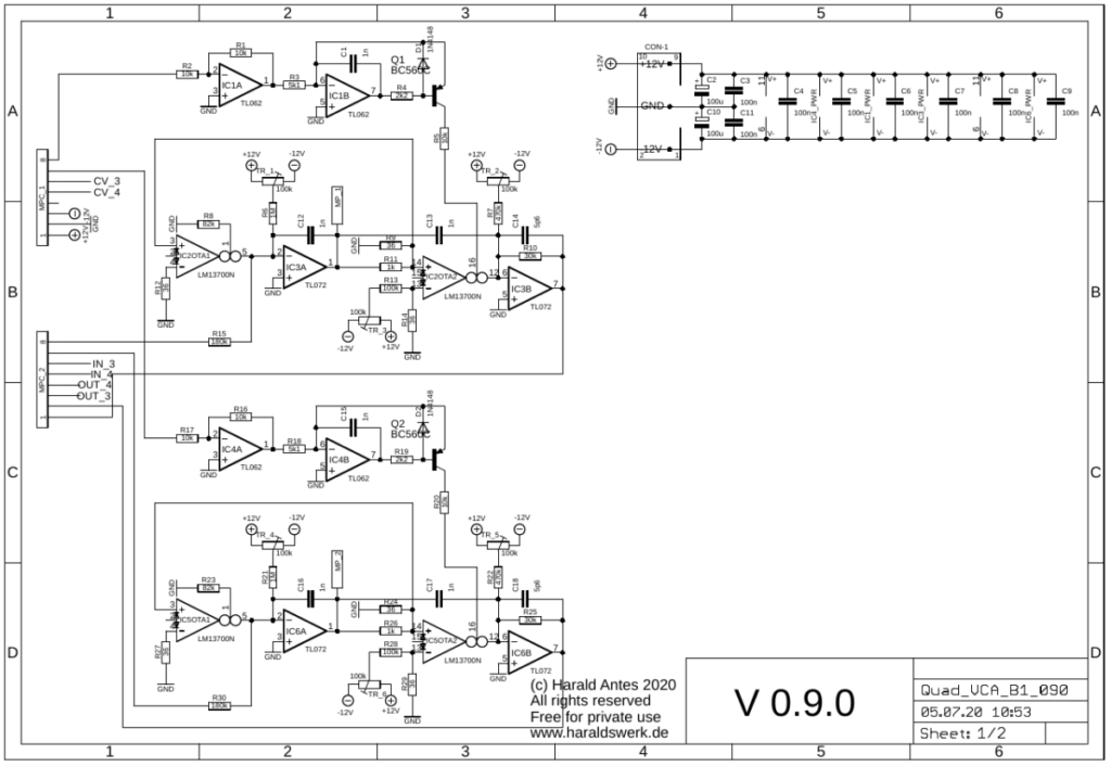
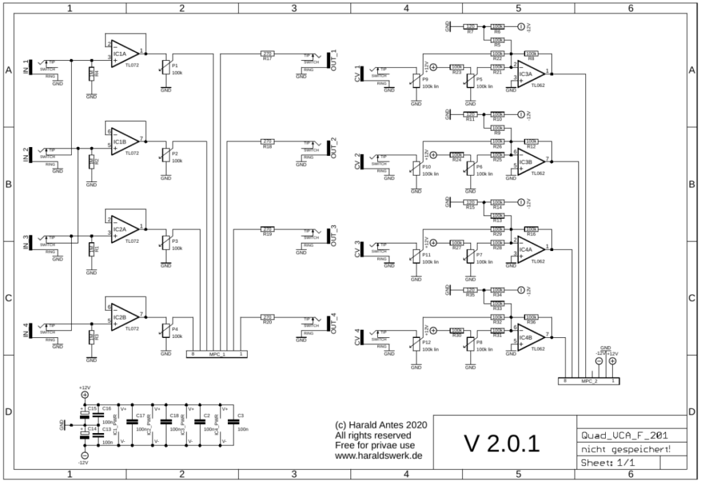
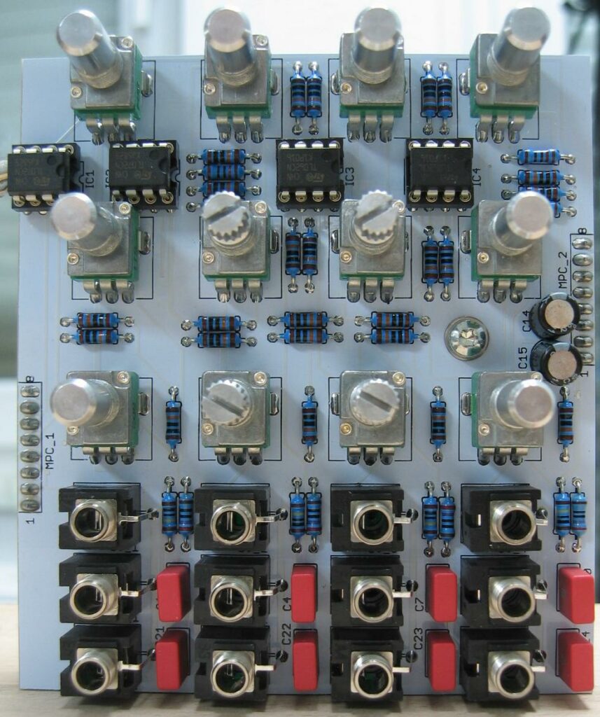
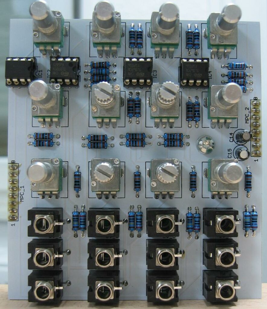
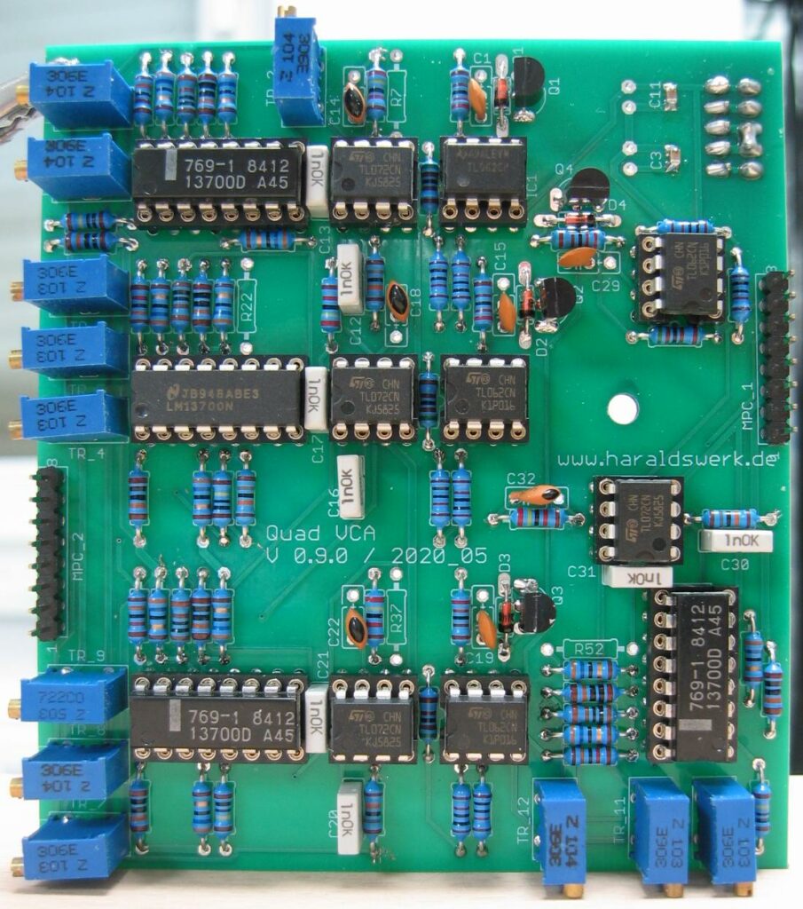
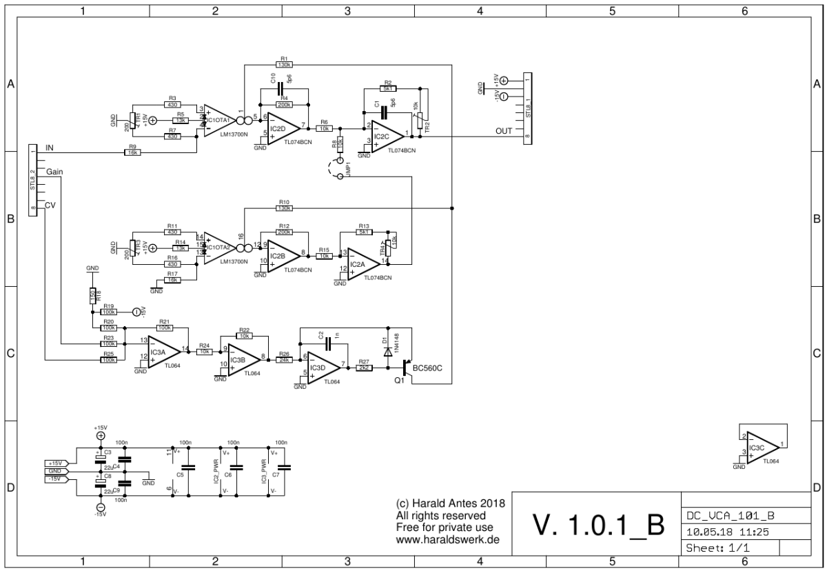
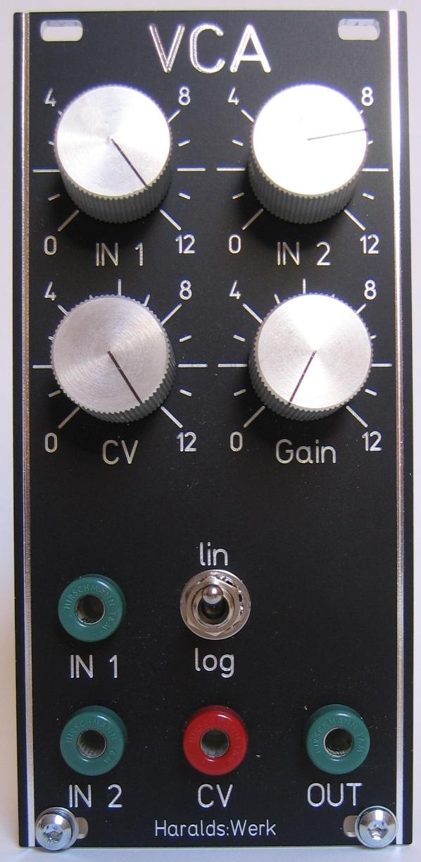
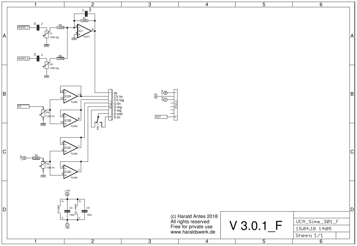
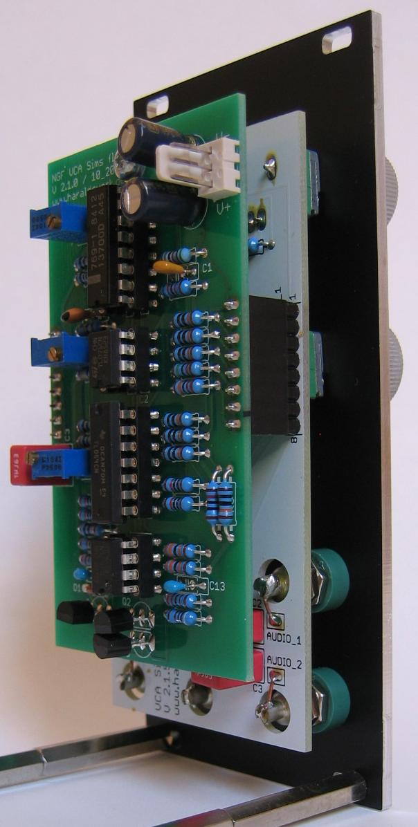
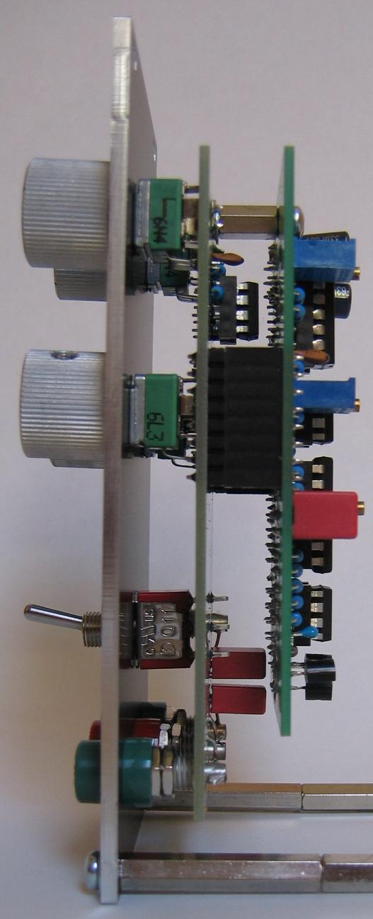
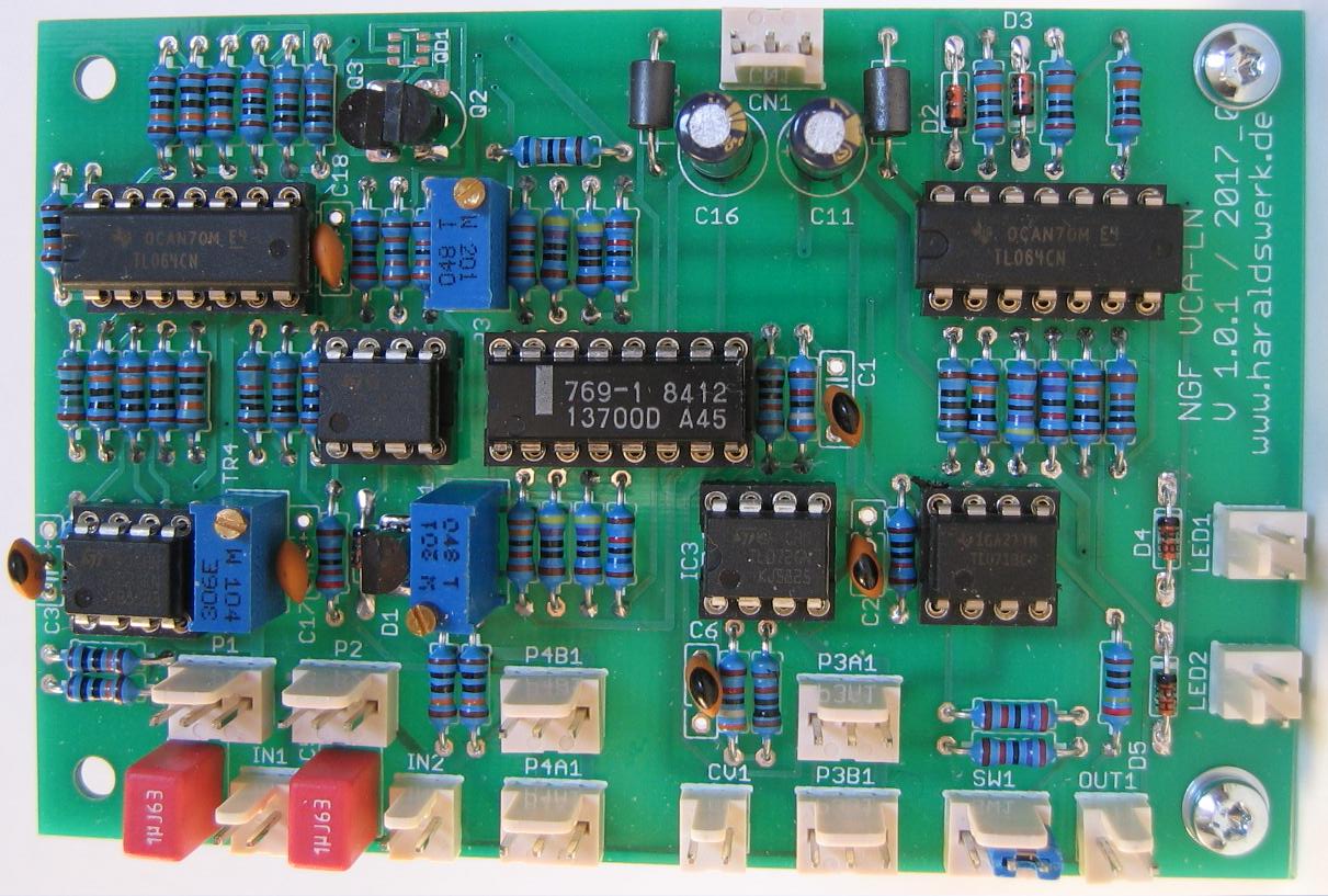
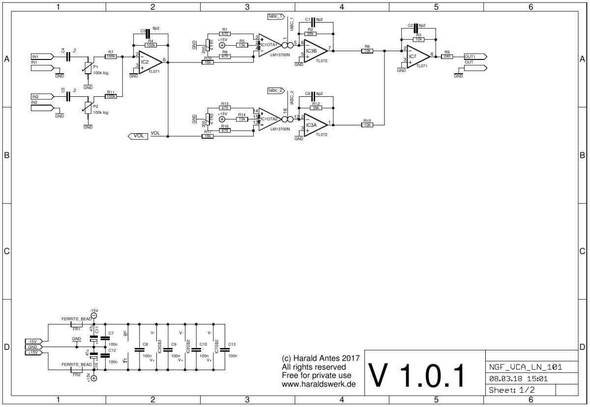
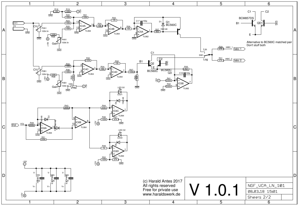
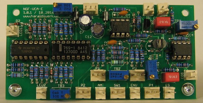
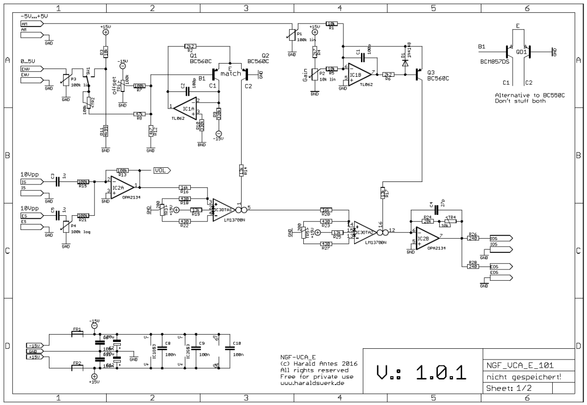
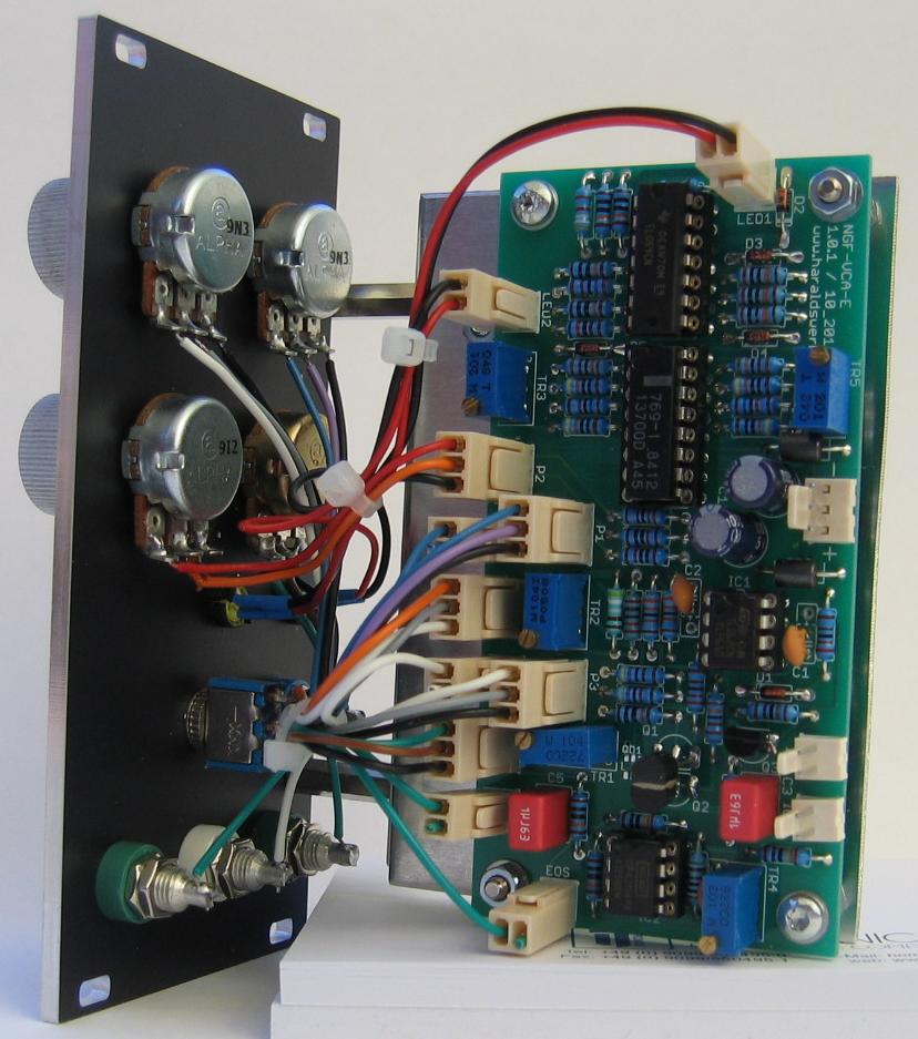
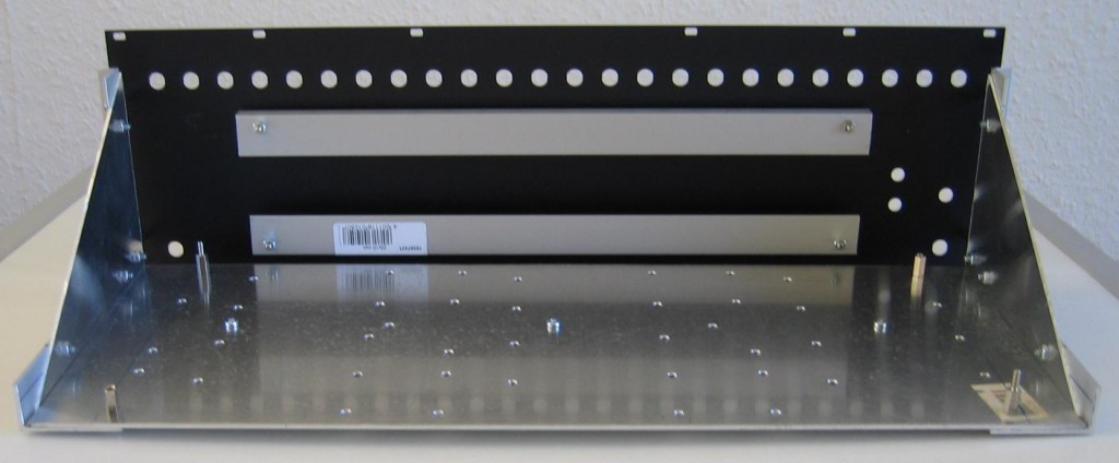
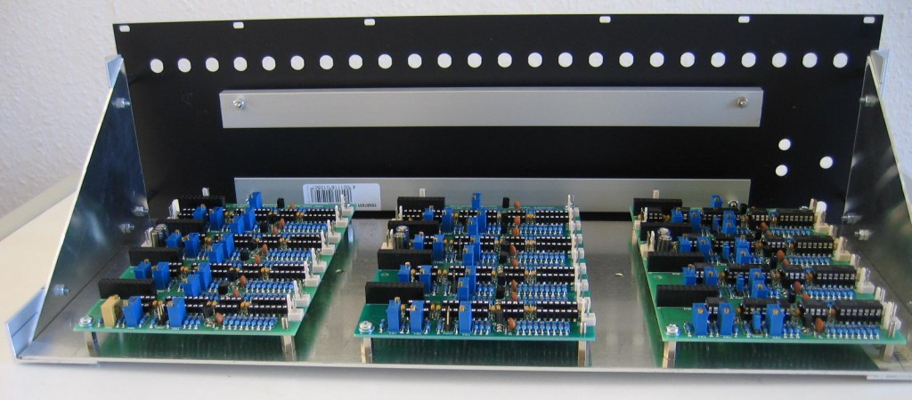
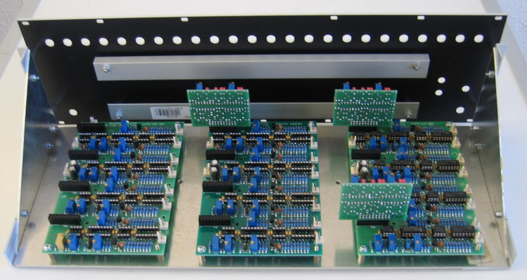
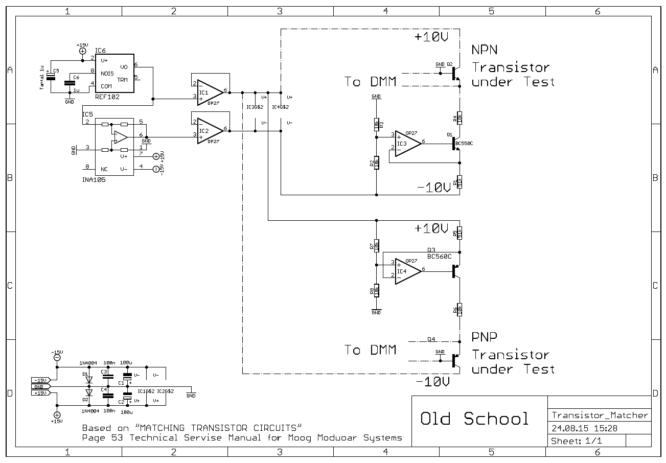
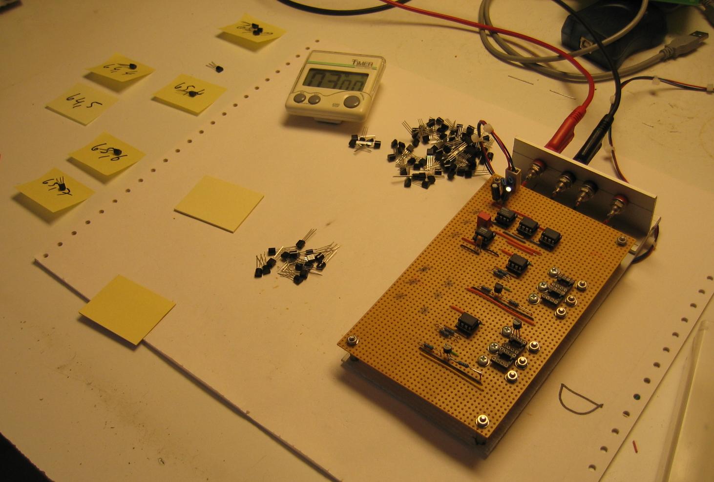
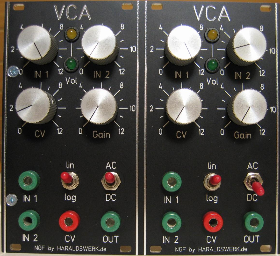
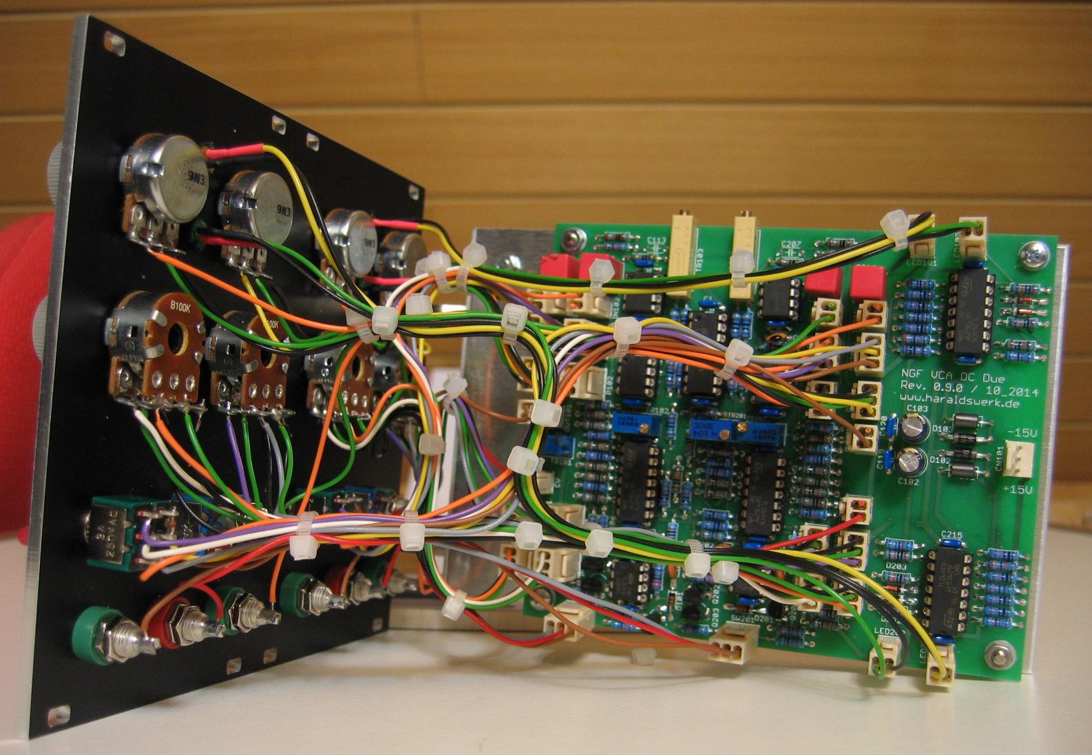
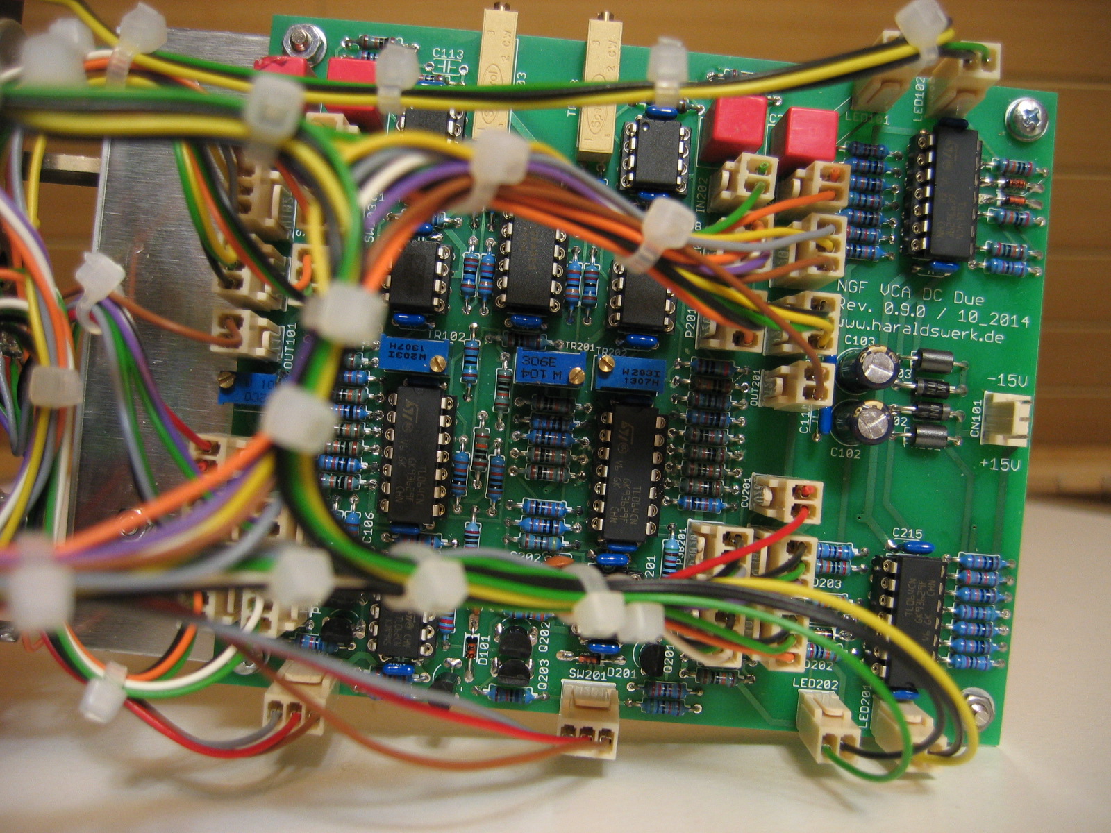
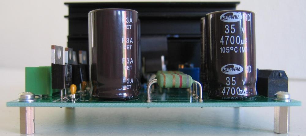
This is the Eurorack version of my Sims VCA. This VCA is AC coupled. I made my own implementation of the Sims-VCA introduced by Mike Sims in the EDN Magazine January 1995. With this architecture it is possible to achieve THD of 0,02%. Unfortunately I can not confirm the statement from Mike Sims that trimming the circuit for minimum THD achieves minimum control voltage feedthrough. Trimming for minimum THD causes an constant DC bias at the output. I have had to add a output capacitor to avoid the bias at the output. And you need test equipment to measure the THD for correct trimming. If you can not measure THD better build my DC-VCA. You can achieve 0,2 % THD there. Still good. Or, for Eurorack, my Quad VCA.
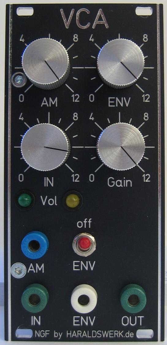
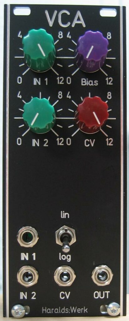
Specs and features

  • AC coupled, 0,02% THD
  • Two inputs
  • Lin and log response
  • CV 0..+5V
  • CV attenuator
  • Adjustable bias
  • Power consumption below 25mA each rail

The documentation and the Gerber files for download can be found in my website.

Sims style VCA: Schematic control PCB
Sims style VCA: Schematic main PCB
Sims style VCA: Populated control PCB
Sims style VCA: Populated main PCB
Sims style VCA: Side view
Sims style VCA: Back view

Quad VCA, AC or DC coupled with normalized input

Quad VCA, AC or DC coupled with normalized input. Front view

This is one more module for my quad system. It contains four VCA with normalized input, so you can distribute one input signal to four output channels. With each channel under voltage control you can move the input signal through the room dependent on the control voltages. I have two versions build one AC and the other DC coupled. Beside using this VCA’s for signal distribution you can use every VCA independently. The gain to voltage ratio is linear. This is done because it is easier to predict the performance. The distribution of the signal must be steered through the control voltages. The implementation follows the recommendations from an article at Open Music Labs from October 3, 2015 (Minimizing distortion in OTA’s)

Specs and features

  • Four VCA with normalized input
  • Usable as four independent VCA as well
  • Linear gain to voltage response
  • Individual Volume, CV and Bias controls
  • Low distortion implementation
  • Runs on +/-12V and +/-15V (with minor resistor value changes for best performance)
  • Power consumption around 35mA each rail

The documentation and the Gerber files for download can be found in my website.

Quad VCA schematic main PCB

The linear controlled current source for Iabc is straight forward and implemented as usual. An elaborate description for the VCA part is given here.

Quad VCA schematic control board DC

On the left side are the potentiometers for volume control followed by the input buffers. The only difference between AC and DC coupling are the capacitors. On the right side are the CV input potentiometers and the bias potentiometers followed by the voltage adder.

Quad VCA control PCB AC coupled
Quad VCA control PCB DC coupled
Quad VCA main PCB
Quad VCA main PCB
Quad VCA back view
Quad VCA back view
Quad VCA side view
Quad VCA side view

DC-VCA / flat Version

DC VCA front view

DC VCA front view

This is the flat Version of my NGF DC VCA. I wanted a decent DC coupled audio VCA to process audio as well as control voltages. And easy available parts (2018/07). I tried different architectures and then decided to separate audio and DC VCA. With specialized VCA it is easier to reach the goal. For control voltage processing I implemented a VCA with active control voltage feedthrough compensation. For lowest control voltage feedthrough you have to use low Iabc as well. So the audio performance is not as good as in my Sims VCA. THD is about 0,2% with selected LM13700. Still not bad and sufficient for DC usage. For DC processing you want to keep the feedthrough and bias of the control input as low as possible. There can be 500mV or more offset depending on the control voltage (I_abc) and it doesn’t vary linearly. There’s a big bump in offset right in the middle of CV range. First thing to do is to lower I_abc to around 250uA. This helps for DC performance but degrades AC performance. The main idea is to use the second OTA of the 13700 to compensate for the CV feedthrough. Both OTA in the 13700 are on the same chip and behaves the same. So I inverted the output of the second OTA and added it to the signal path. You still have to select the LM13700 for best performance.

Specs and features:
• DC coupled
• Active CV feedthrough compensation
• Linear response
• CV 0..+5V
• 5Vpp in- and output
• Positive and negative output
• Runs on +/-15V and +/-12V
• Power consumption below 20mA each rail

The documentation for download can be found in my website.

VCA DC schematic back PCB

VCA DC schematic back PCB

VCA DC schematic front  PCB

VCA DC schematic front PCB

On the top is a plain forward implementation for an VCA. Next row is the same VCA with input set to ground and output inverted. The inverted output of the second VCA is added to the output of the first one to compensate for the CV feedthrough. The output voltage is adjusted with TR2/TR4 for different Gm off OTA’s.

VCA DC side view

VCA DC side view

VCA DC left view

VCA DC left view

VCA DC back view

VCA DC back view

VCA Sims / flat Version

VCA Sims - flat Version

VCA Sims – flat Version

This is the flat Version of my Sims VCA. The original Elektor Formant VCA used two 3080 in series. In most cases only one is used and the second one only adds to noise and distortion. This VCA is AC coupled only. The THD in the Elektor Formant VCA is about 1% and the noise to voltage ratio is not that good either. Time to look for a replacement. I wanted a decent DC coupled audio VCA to process audio as well as control voltages. And easy available parts (2014/08). I tried different architectures and then decided to separate audio and DC VCA. With specialized VCA it is easier to reach both goals. I made my own implementation of the Sims-VCA introduced by Mike Sims in the EDN Magazine January 1995. With this architecture it is possible to achieve THD of 0,02%. Unfortunately i can not confirm the statement from Mike Sims that trimming the circuit for minimum THD achieves minimum control voltage feedthrough. Trimming for minimum THD causes an constant DC bias at the output. I have had to add a output capacitor to avoid the bias at the output. And you need test equipment to measure the THD for correct trimming. If you can not measure THD better build my DC_VCA. You can achieve 0,2 % THD here. Still good.

Specs and features:
• AC coupled 0,02% THD
• lin and log response
• CV 0..+5V
• 5Vpp in- and output

The documentation for download can be found in my website.

VCA Sims schematic back PCB

VCA Sims schematic back PCB

VCA Sims schematic front PCB

VCA Sims schematic front PCB

Please refer to my first implementation (link) or the original article from Mike Sims

VCA Sims side view

VCA Sims side view

VCA Sims side view

VCA Sims side view

VCA LN

VCA LN: populated PCB

VCA LN: populated PCB

A well known way to reduce noise in VCA is using the VCA’s in parallel. Here is my approach. A LM13700 used in parallel reduces the noise floor around 3dB.
Specs and features
• VCA with reduced noise floor
• Runs on +/-15V and +/-12V (with some resistors changed)

The documentation for download can be found in my website.

VCA LN: Schematic 01

VCA LN: Schematic 01

Nothing special here. Just two plain forward designed VCA with LM13700. With the signals added together.

VCA LN: Schematic 02

VCA LN: Schematic 02

Standard circuitry for Iabc and level control.

NGF-E Project: VCA

NGF-E Project: VCA stuffed PCB

NGF-E Project: VCA stuffed PCB

This is my take on the VCA. Because this one is for my Next Generation Formant project i started with the original Elektor Formant VCA schematic and added my changes to the design. All parts are updated to today (2017/08) available parts. The connections are the same as in the original to keep the possibility for internal wiring. If you don’t need those features just leave them out. This PCB provides all functions as in the original Elektor Formant VCA. The CA3080 are replaced with LM13700. The signal level is raised to 10Vpp for a better signal to noise ratio. The added volume indicator us useful for finding the appropriate signal level. The volume indicator is optional. You can leave it out with no problems for the other functions.

The documentation for download can be found in my website.

NGF-E Project: VCA schematic

NGF-E Project: VCA schematic

This is a close clone of the Elektor Formant VCA. It consists off two OTA’s in serial configuration. The first OTA provides the log response and the second one the linear response. IC2A sums up the external and internal audio signal. The circuitry around IC1A provides the log converter, IC1B the linear current source for the second OTA.
Calibration procedure and more information on my website.

NGF-E Project: VCA front view

NGF-E Project: VCA front view

NGF-E Project: VCA back view

NGF-E Project: VCA back view

Vocoder: Synthesizer VCA’s


Vocoder: Syntesize Part VCA

Vocoder: 24Channels Synthesize Part VCA

Here are the VCA’s of the synthesize part from my Vocoder project. I followed the same modular principle as in the other parts of the Vocoder. Each VCA PCB contains 8 VCA channels. So you can start with 8 channels and advance to 16 or 24 channels. The VCA’s are designed plain forward around the LM13700 as commonly used. The output voltage for each VCA is adjustable to compensate different gain from the filters. The filters are pluggable as in the analyze part. You have the opportunity to swap filters around and test different filter topologies. The schematic given here contains only two channels. The complete documentation will show up on my website when everything is finished. Next to come: The filters for the synthesize part.

Vocoder: Synthesize Part PCB 8 Channels stuffed.

Vocoder: Synthesize Part PCB 8 Channels stuffed.

Schematic shows only two channels. Complete documentation on my website asap.

Vocoder: Synthesize Part Schematic VCA

Vocoder: Synthesize Part Schematic VCA

Vocoder: Synthesizer mechanic

I am in the process of completing the synthesizer part of my vocoder project. So far I have the faceplate, the mechanic, the VCA part and a few filters ready. Still a lot of work ahead. Stuffing all the filter PCB and trimming, doing the voiced/invoiced detection, input/output section, exciter part and housing. Here are some pictures.


Faceplate and the mechanical parts sawed and drilled.

Vocoder: synthesizer mechanic

Vocoder: synthesizer mechanic parts ready

Waiting for PCB.

Vocoder: Synthesizer mechanic parts mounted

Vocoder: Synthesizer mechanic parts mounted

Vocoder: Synthesizer mechanic back

Vocoder: Synthesizer mechanic back

Does the VCA PCB fit for the Vocoder fit?

Vocoder: Synthesizer VCA PCB mounted

Vocoder: Synthesizer VCA PCB mounted

Some Filters to the Vocoder added.

Vocoder: Synthesizer VCA with some filters added

Vocoder: Synthesizer VCA with some filters added

Tool: Transistor Matcher

Matched transistor-pairs are often needed while building modules for synthesizers. Especially for exponentiators and differential amplifiers. Not to forget the Moog style ladder filters. I build an transistor matcher for me many years ago and still use it. I know that there are easier matching circuits out there today but mine works great for me so there is no need to change. Mine is based on the original transistor matcher found in the “Technical Service Manual for Moog Modular Systems” on page 53. I added some circuitry for stabilizing the used voltages. That was done to be able to repeat the measurement without bothering about the power supply adjustment. We are dealing with 1mV – 2mV here!

Transistor Matcher schematic

Transistor Matcher schematic


There was no need for a PCB. I just put it on perfboard and used IC sockets for the DUT.

Transistor Matcher

Transistor Matcher


The usage is easy but you have to consider some precautions. The measurement is very temperature sensitive. You need to keep your environment stable. Use pliers to mount the DUT. Place the transistors into the socket. Measure base to emitter voltage. Don’t touch the transistors with fingers. The finger heat will cause the readings vary. Mark down the Vbe and find two transistors that the Vbe matches within 2mV or better.

Transistor Matcher usage

Transistor Matcher usage


With today standards of fabrication transistors it is not unusual to find nearly every transistor within the 2mV Vbe range in a batch. You can easily match your pairs to better standards. Depending on your equipment 0.5mV Vbe match should be easily to reach. But always remember: The measurement is very sensitive. Be careful with your setup!

VCA with low CV feedthrough again

As said in my last post it is to much effort to use active CV feedthrough compensation for the result and to use the second LM13700 OTA for a second VCA. Meanwhile the PCB and the faceplate for my http://www.haraldswerk.de/NGF/NGF_VCA_DC_due/NGF_VCA_DC_due.html arrived.

20141112_01

After stuffing the PCB I selected an LM13700 OTA for best DC performance. As expected the DC performance was good. About 2mV CV feedthrough over the whole 5V range with a THD of 0,2%. But wait….. there is an second OTA as well. My assumption was both OTA behave the same because they are on the same die. Nope. I was wrong! The second VCA shows a CV feedthrough of 7mV over the 5V range. Not that good.

20141112_02

It is hard enough to find an LM13700 OTA with low CV feedthrough but it will be a lot harder to find an OTA where both sides behaves the same. This explains some trouble I have had with the active feedthrough compensation as well.

So I skip the idea to use both OTA in the LM13700 for VCA with low CV feedthrough. The way to go is to select the chip for one “good” site and leave the other site alone. Not a big deal, they are not that costly. I’ll do it with my next VCA the NGF VCA DC one.

If I find the time I will put up a test circuit to find an LM13700 with identical behavior on both sites and use it in my active feedthrough compensation design to see if I can do better then 1mV feedthrough.

20141112_03