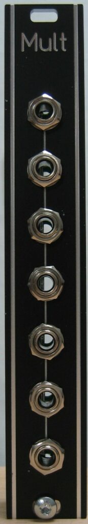
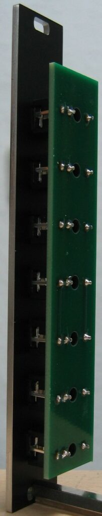
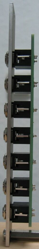
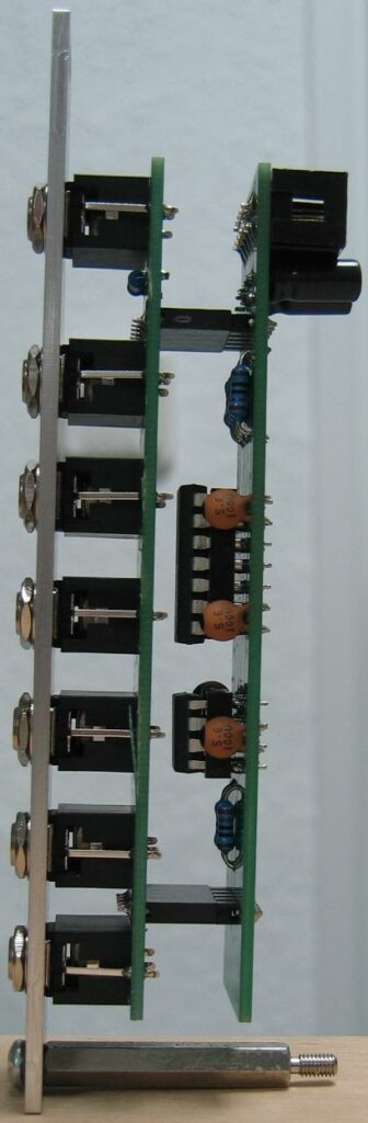
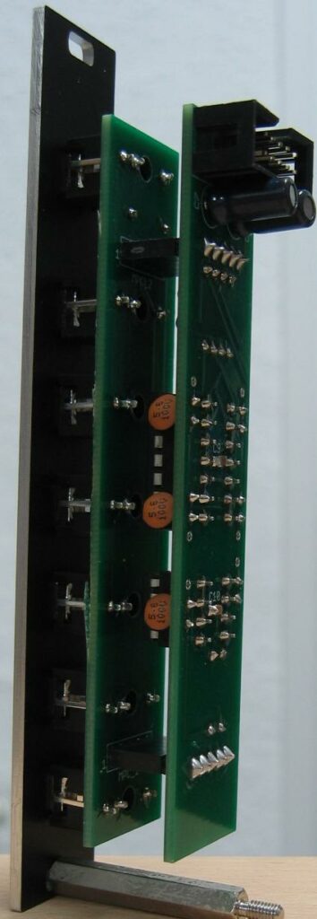
Just another often needed utility module. A passive multiple.
Specs and features
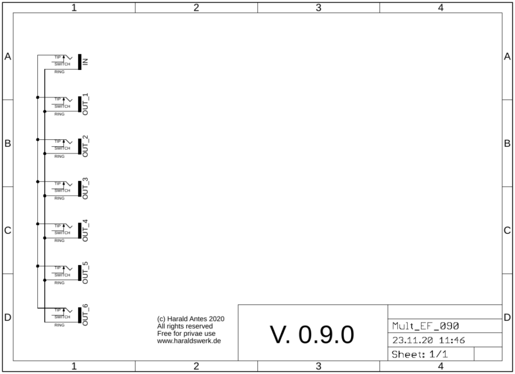
- Seven passive parallel in/outs
- No power connection
The documentation and the Gerber files for download can be found in my website.
Just another often needed utility module. A passive multiple.
The documentation and the Gerber files for download can be found in my website.
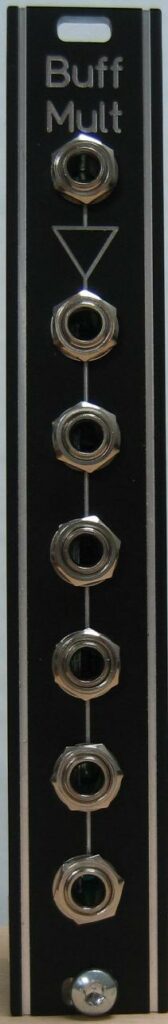
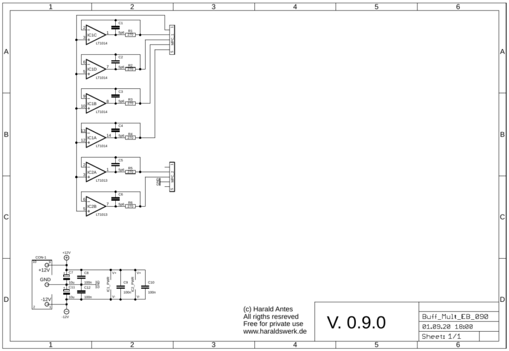
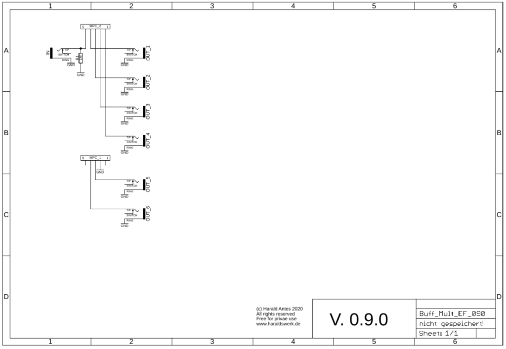
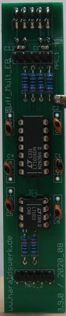
This is a useful and often needed utility module. The input voltage is precisely reproduced on the outputs. It comes in handy when you need to distribute signals which must be decoupled. The input signal is buffered and decoupled with means of individual operational amplifiers. One input drives 6 individual outputs. The accuracy depends on the used operational amplifier. For pitch CV I recommend precision OpAmps like the LT1014 (quad) and LT1013 (dual).
The documentation and the Gerber files for download can be found in my website.
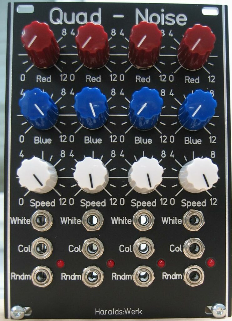
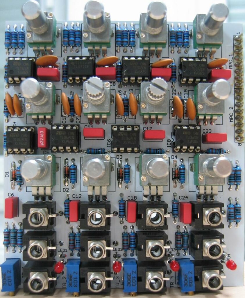
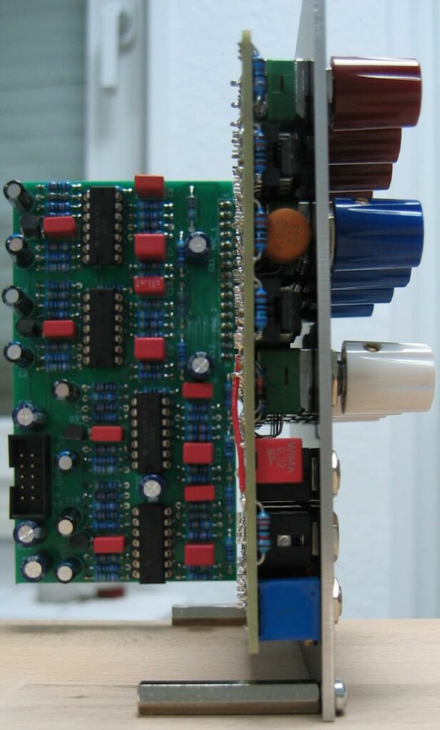
It is quite useful to have different adjustable noise and random voltage sources. Depending on your patch stile of course. Here is the quad version of my noise module from the NGF project. It is a combination of two original Elektor Formant modules. The noise module from Elektor Formant book one and the colored noise (CNC) module from book two. It provides four independent white noise outputs, four adjustable colored noise outputs with “red” and “blue” adjustment. The four random voltage outputs are adjustable in speed of change. The noise is derived from the reverse biased BE diode of an NPN transistor.
The documentation and the Gerber files for download can be found in my website.
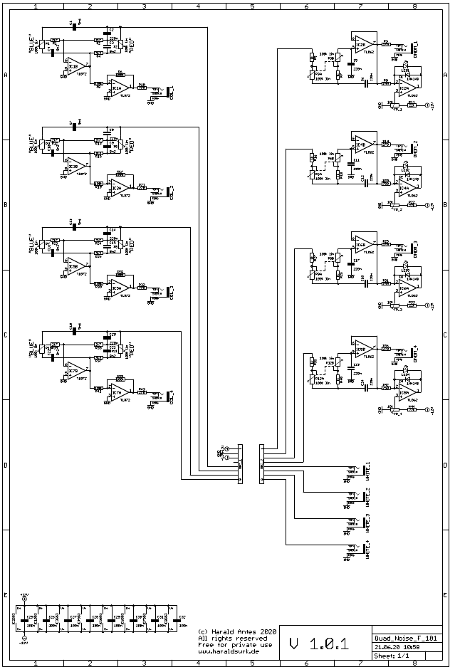
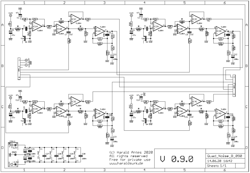
(Given for one of the four.) Noise source is the reverse biased BE diode of NPN transistor Q1 (B_090). The following operational amplifier IC1A and IC1B (B_090) amplifies the noise to 10Vpp. IC1C (B_090) is the buffer for the white noise output. IC2B (F_101) is configured as a 12dB low pass. So you get a low frequency random voltage. The changing speed is set with P3A/P3B (F_101) which sets the corner frequency of the low pass filter. IC2A / LED1 (F_101) makes the fluctuation visible. TR_1 (F_101) adjust the brightness of LED1 (F_101). In the feedback loop of IC1B (F_101) is an adjustable filter combination which gives you a wide range of adjustable colored noise with P1 and P2 (F_101). The output is buffered with IC1A (F_101).
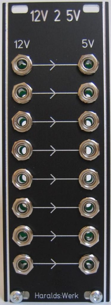
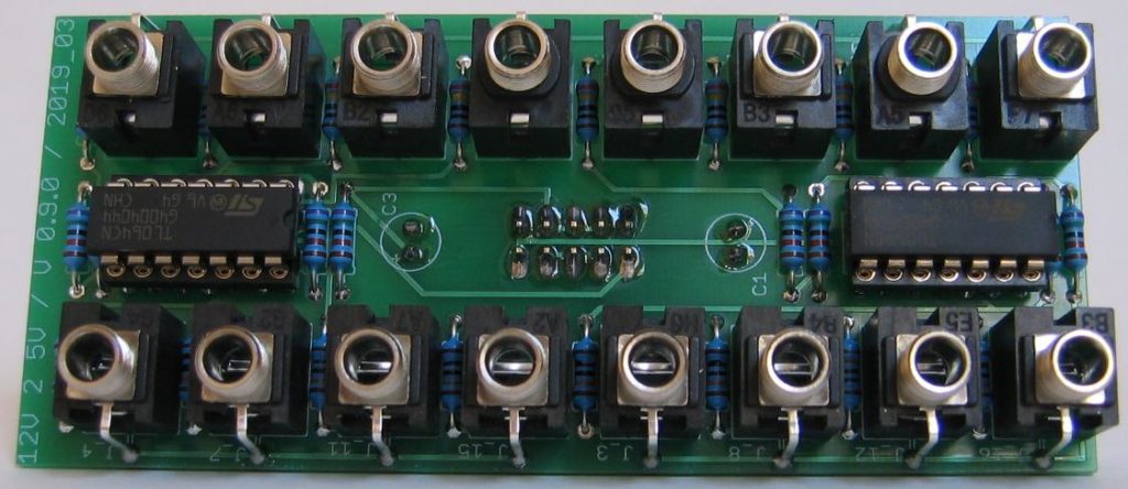
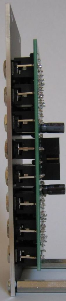
This utility module converts a 12V gate to a 5V gate. It is needed when you have a module with 12V gate output and your receiving module only accepts 5V gate voltage.
The documentation and the Gerber files for download can be found in my website.
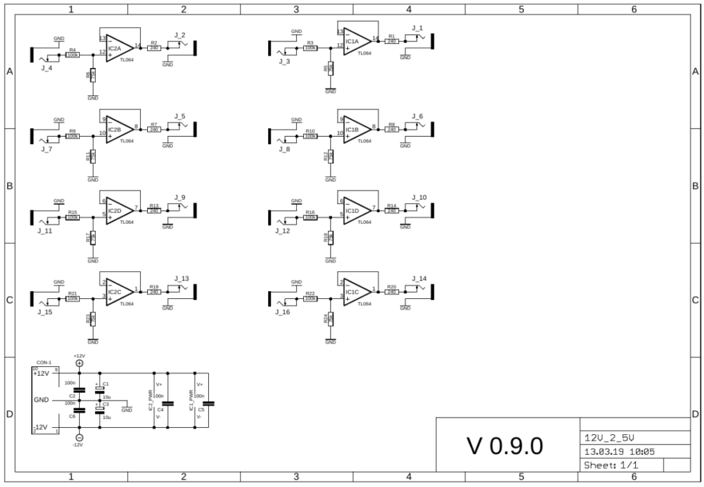
The 12V input is divided down with the input voltage divider to 5V and buffered.
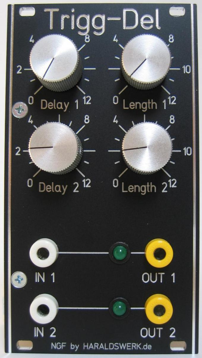
Trigger Delay front
This module can delay an incoming trigger signal up to 8 seconds. The trigger length is adjustable up to 8 seconds as well. The trigger pulse length is independent from the input signal length. Both parameters are independently adjusted with potentiometers. The output state is shown with a LED.
Specs and features
• Input: positive Trigger or any fast changing voltage.
• Output: 5V pulse with adjustable delay and length.
• PSU +15V/-15V or +12V/-12V
The documentation for download and the Gerber files for download can be found in my website.
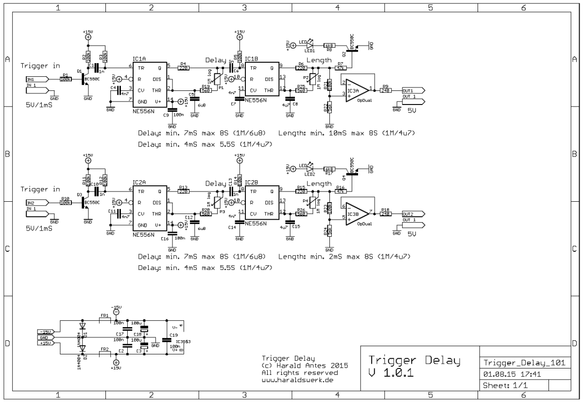
Trigger Delay schematic
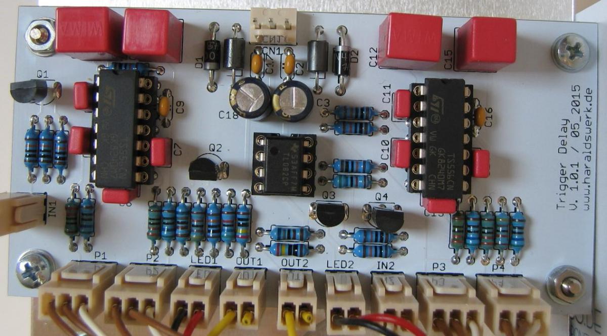
Trigger Delay populated PCB
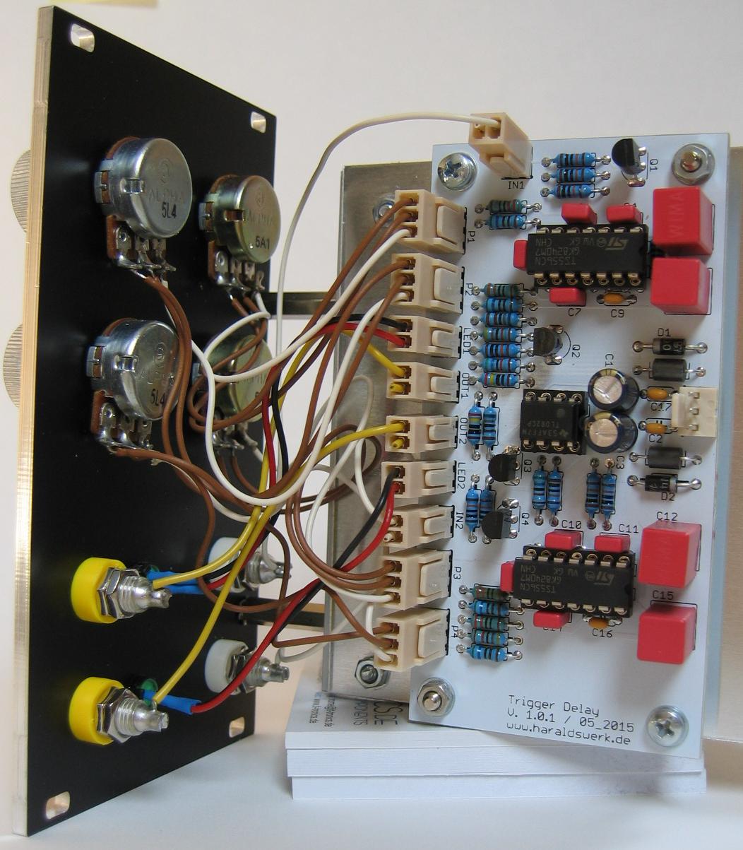
Trigger Delay back view
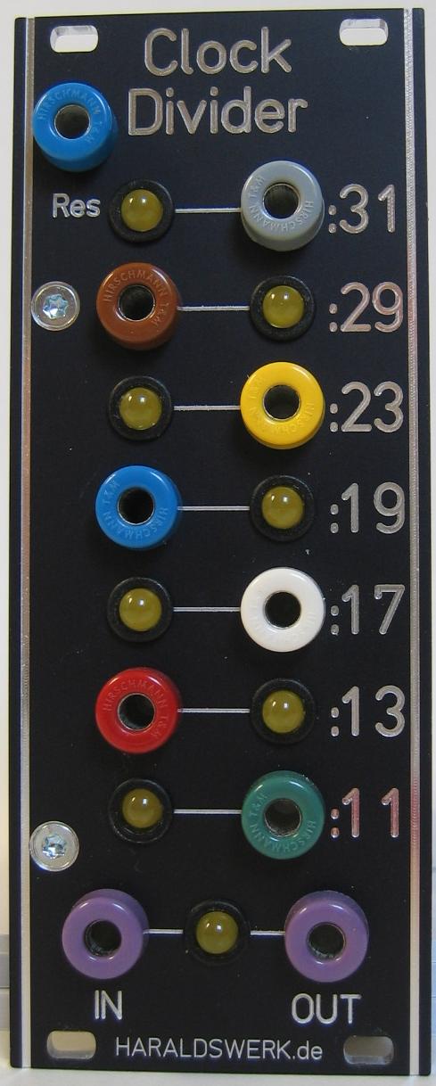
Clock Divider with prime numbers
This clock divider divides the incoming clock signal down to the prime numbers /11, /13, /17, …. /31. The output is a 5V positive pulse. The length of the incoming pulse is kept. The trigger is on the rising edge of the incoming signal. The reset input can be used for syncing with other clocks. All outputs are buffered and brought out parallel with LED signaling the pulse.
Specs and features
• Regular input clock/square wave +5V
• Input signal divided by prime numbers
• Output +5V pulse with the length of the input signal (pulse)
• Runs with +15V/-15V or +12V/-12V (with minor changes)
The documentation for download can be found in my website.
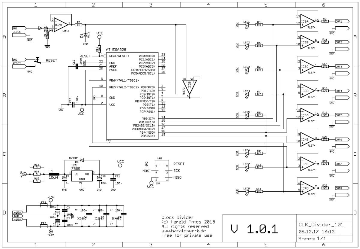
Clock Divider with prime numbers, schematic
Most work is done by the microprocessor. The micro takes care of the input and output timing. All outputs are independently buffered. The clock is made visible with LED.
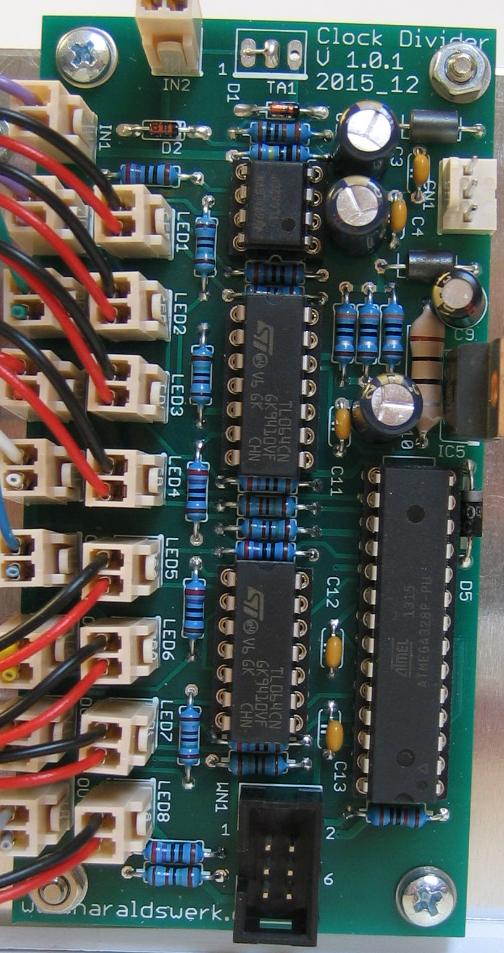
Clock Divider with prime numbers, populated PCB
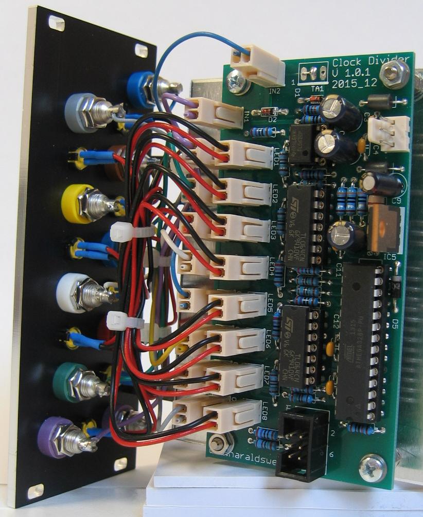
Clock Divider with prime numbers, rear view
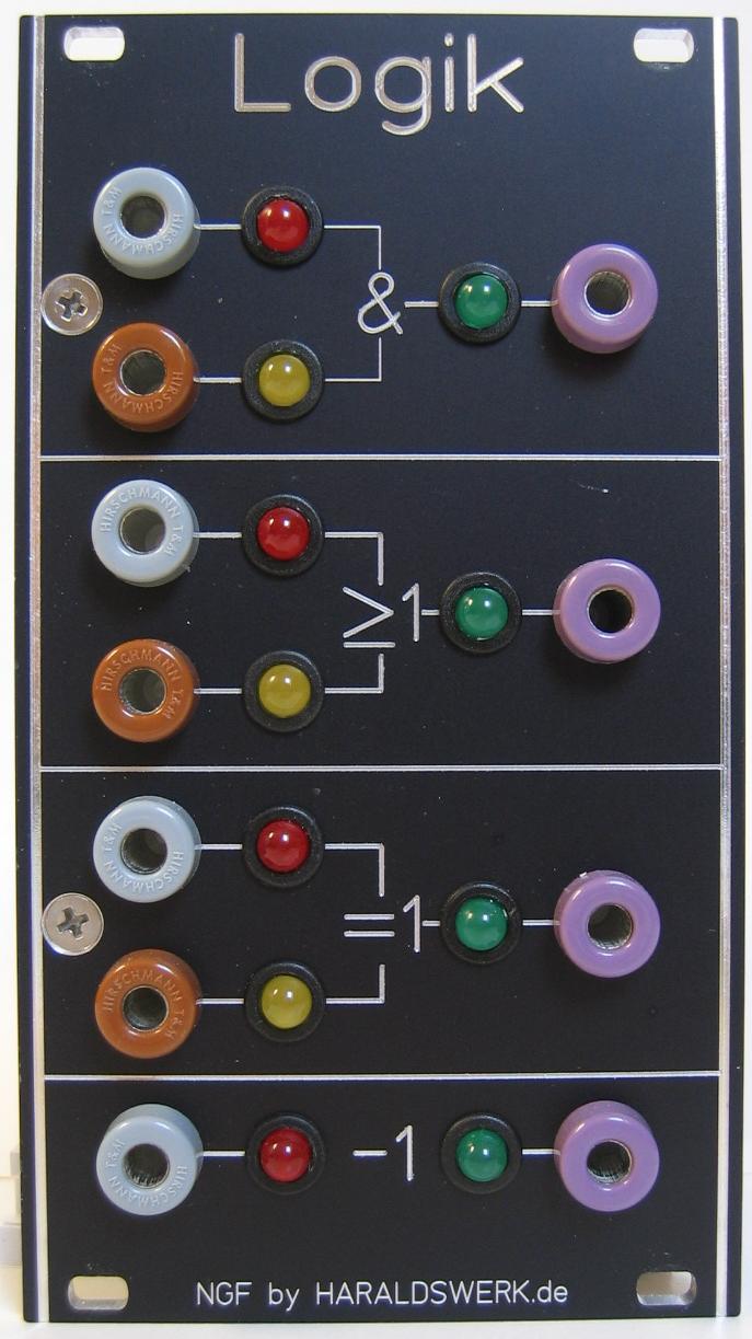
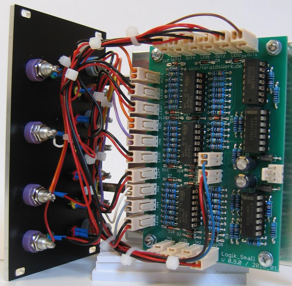
Logic Module front
I needed a module to combine gate and/or trigger events for steering sequencers, ADSR and other gear. So I build one. This one here has and, or, ex-or and neg logic gates. The states of the inputs and output are signaled with LED. The inputs takes audio as input as well. This makes for some interesting patches. The minimum input level can be set to your needs.
The documentation for download can be found in my website.
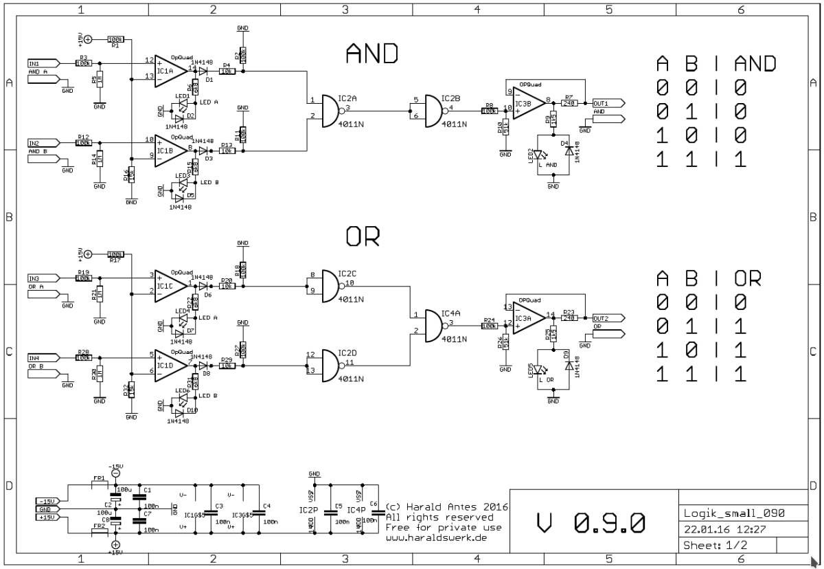
Logic Module schematic p. 01
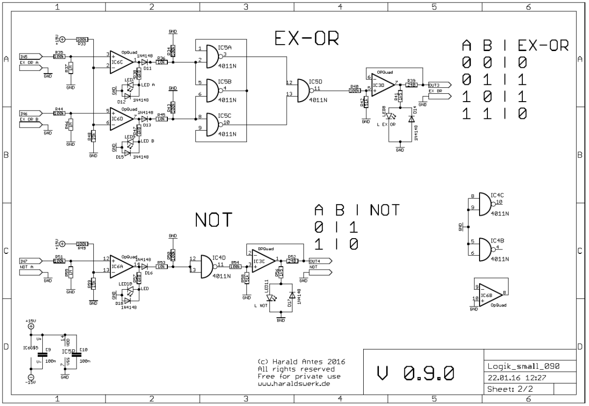
Logic Module schematic p. 02
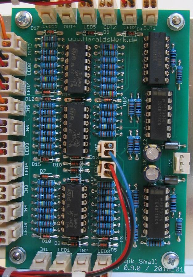
Logic Module populated PCB
Logic Module back view
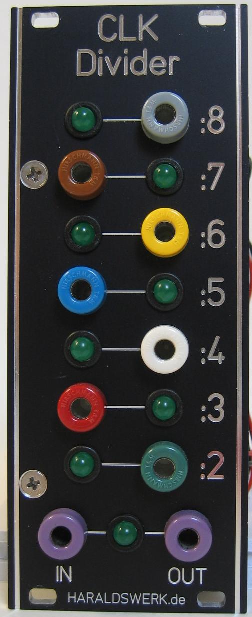
Clock Divider 2-8 front view
This clock divider divides the incoming clock signal down to /2, /3, …. /8. The output is a 5V positive pulse. The length of the incoming pulse is kept. The trigger is on the rising edge of the incoming signal. The reset input can be used for syncing with other clocks. All outputs are buffered and brought out parallel with LED signaling the pulse.
The documentation for download can be found in my website.

Clock Divider 2-8 schematic
Most work is done by the microprocessor. The micro takes care of the input and output timing. All outputs are independently buffered. The clock is made visible with LED.
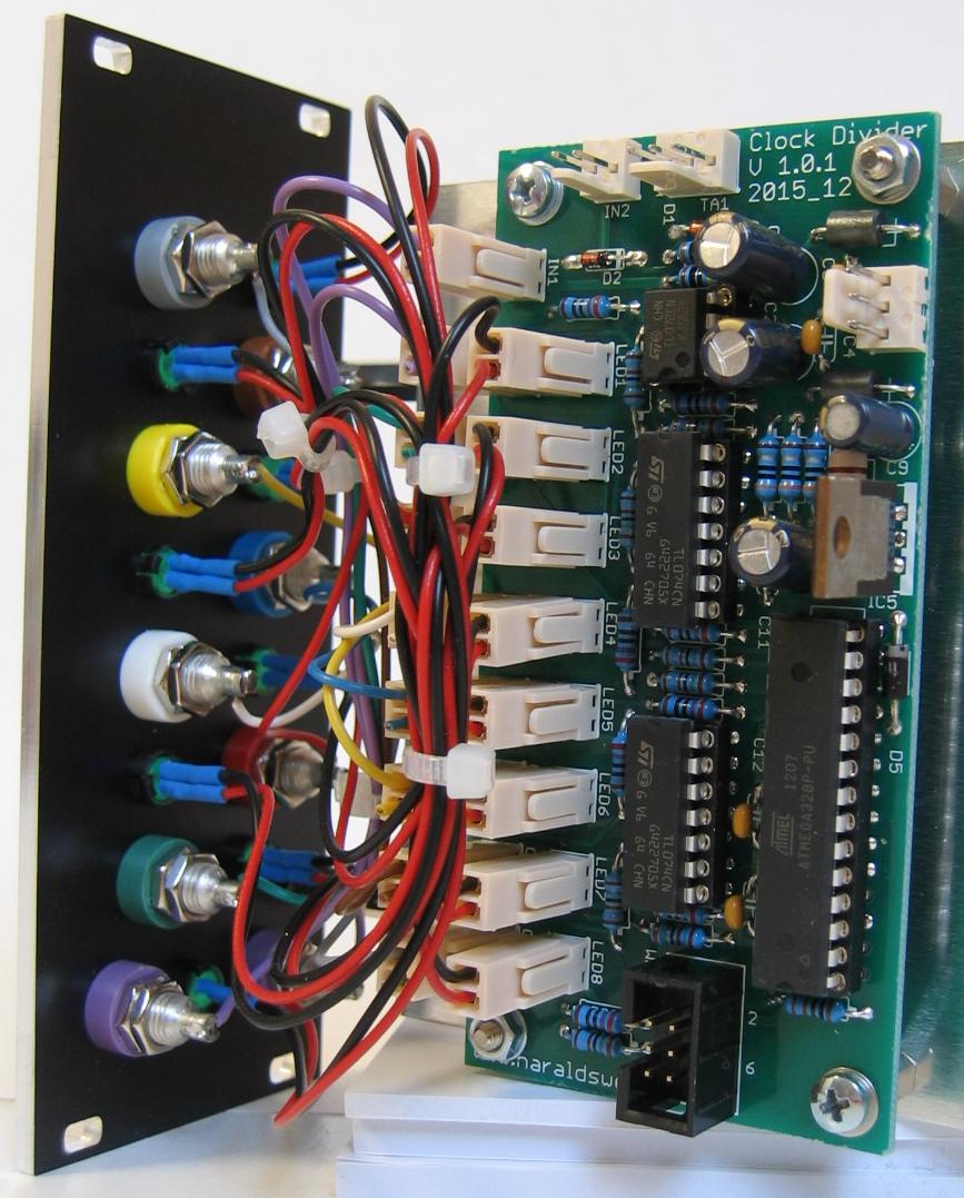
Clock Divider 2-8 back view
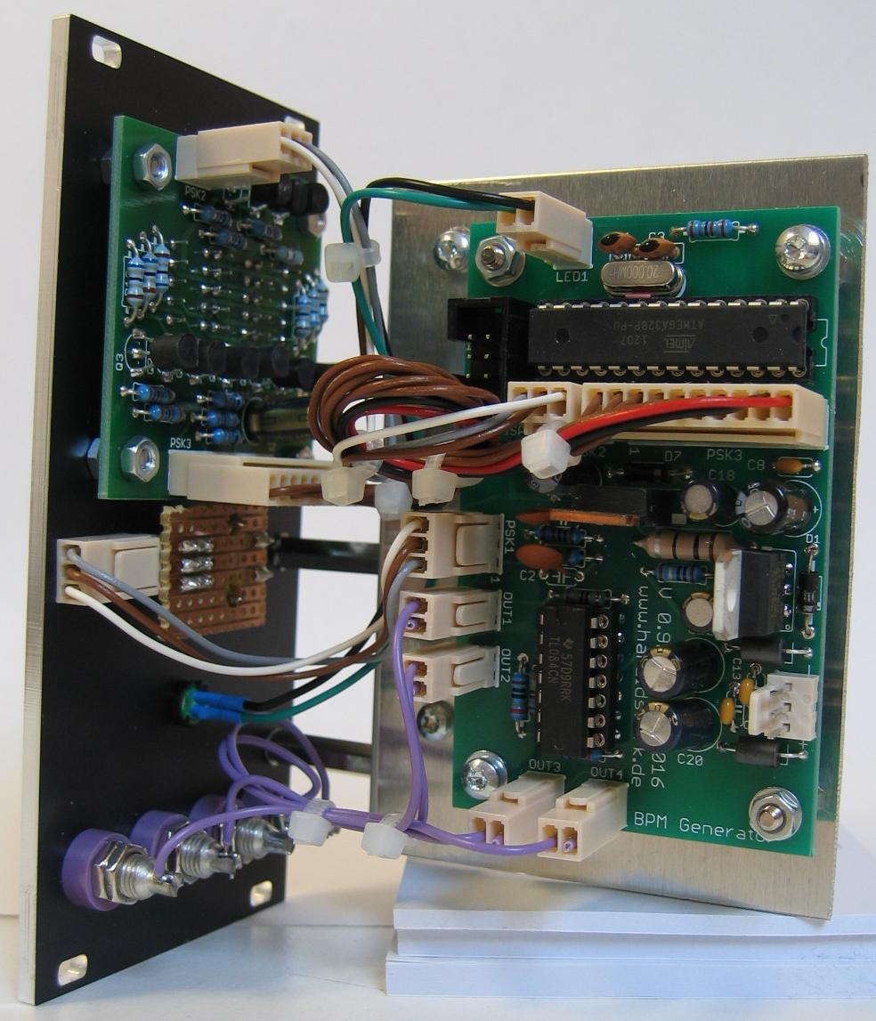
BPM Generator module back
The BPM Generator give you +5V pulses output with 20ms length, from 40 to 240 beats per minute. Controlled by a microprocessor. The BPM are displayed with three 7 segment LED. The speed is adjusted with an rotary encoder.
The documentation for download can be found in my website.
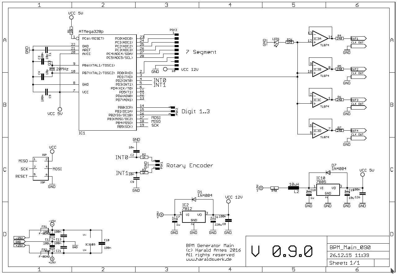
BPM Generator module schematic main
Most work is done by the microprocessor. The micro takes care of the output timing and the multiplexing off the display. All four outputs are independently buffered.
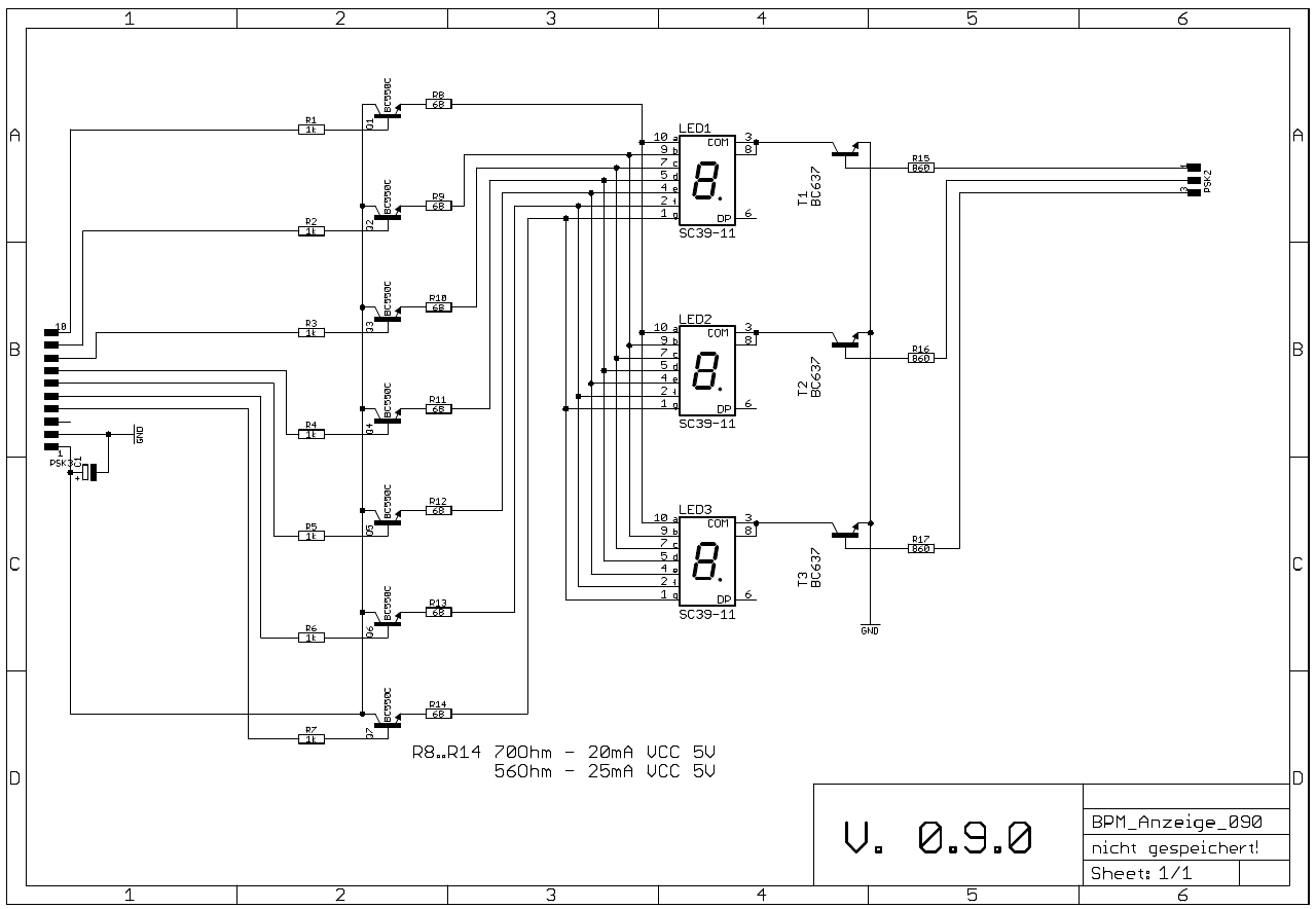
BPM Generator module schematic display
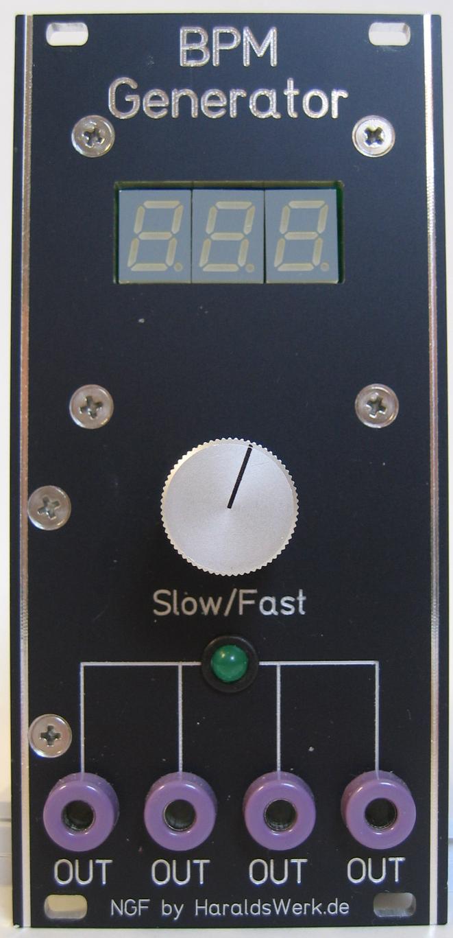
BPM Generator module front
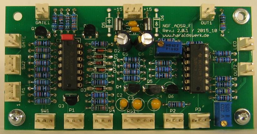
NGF-E Project: ADSR stuffed PCB
This is my take on the ADSR. Because this one is for my Next Generation Formant project i started with the original Elektor Formant ADSR schematic and added my changes to the design. All parts are updated to today (2017/09) available parts. The connections are the same as in the original to keep the possibility for internal wiring. If you don’t need those features just leave them out. This PCB provides all functions as in the original Elektor Formant ADSR. I have made a few changes to fix some shortcomings of the original. A triple range switch was added for finer adjustment of the ADSR CV-output signal. The attack rise time is shorter now as in the original. The gate input is buffered. The fixes a fault in the original when working with analog sequencers. The output voltage is slightly raised to reach really 5V. Due to the design of the original Elektor Formant ADSR the output of the original ADSR keeps a residual voltage of about 0,5V. I have put an adjustable compensation in my design to correct this and keep the original behavior if needed as well.
The documentation for download can be found in my website.
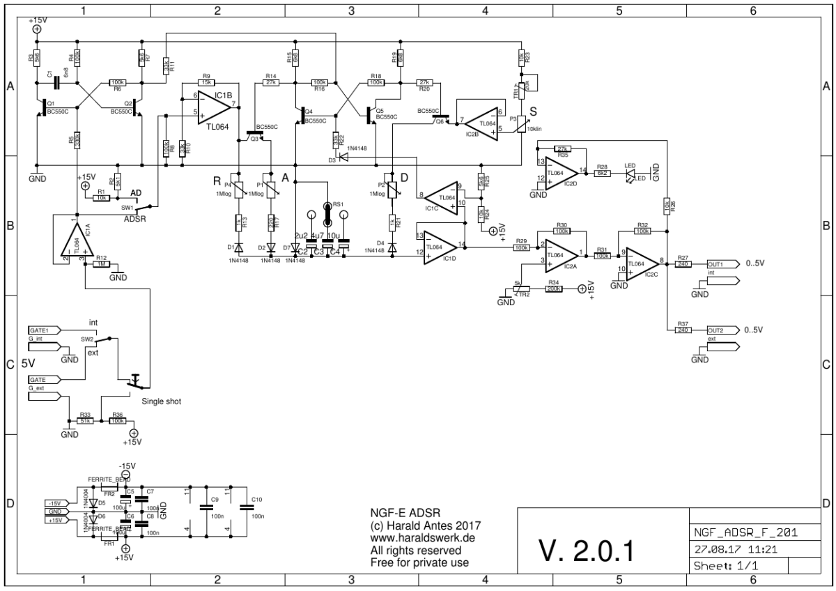
NGF-E Project: ADSR schematic
This is a close clone of the Elektor Formant ADSR. Here i only describe the changes i have made. The description of the other parts of the circuitry can be found in the original Elektor Formant documentation. The gate signal input resistance is raised from 33kOhm to 1megOhm with the input buffer IC1A. This protects against double triggering with the falling edge of the gate signal when using sequencers. R12 is used to fix the input to a defined potential when no signal is attached to the input. R33 and R36 in combination with a push button give you the single shot feature. C1 was lowered to 6n8 from 10nF. In combination with C2 and the raised charging voltage through IC1B/R9 this makes for faster attack time. The load capacitor of 10u was replaced with three selectable capacitors of 2,2uF 4,7uF and 10uF. This make for a finer adjustment of the response times of the ADSR. The voltage divider R24/R25 was adjusted to ensure that the output level of 5V is reached when the offset option with TR2 is used. If this feature is not used R25 should be lowered to 5k1. Construction conditioned the output at IC1D only reaches a minimal voltage of about 0,5V. To compensate for this i added IC2C. With TR2 you can trim the output down to zero volts. If the ADSR is not used the output voltage is now at -0,5V. If you don’t want to use this feature just turn TR2 to ground and you will have the original behavior of the original Elektor Formant ADSR. The current consumption was lowered with using the TL064 and a low current led.
Calibration procedure and more information on my website.
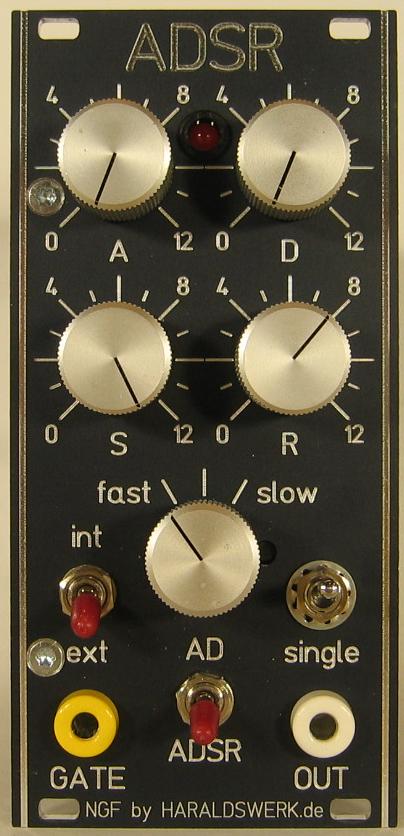
NGF-E Project: ADSR faceplate
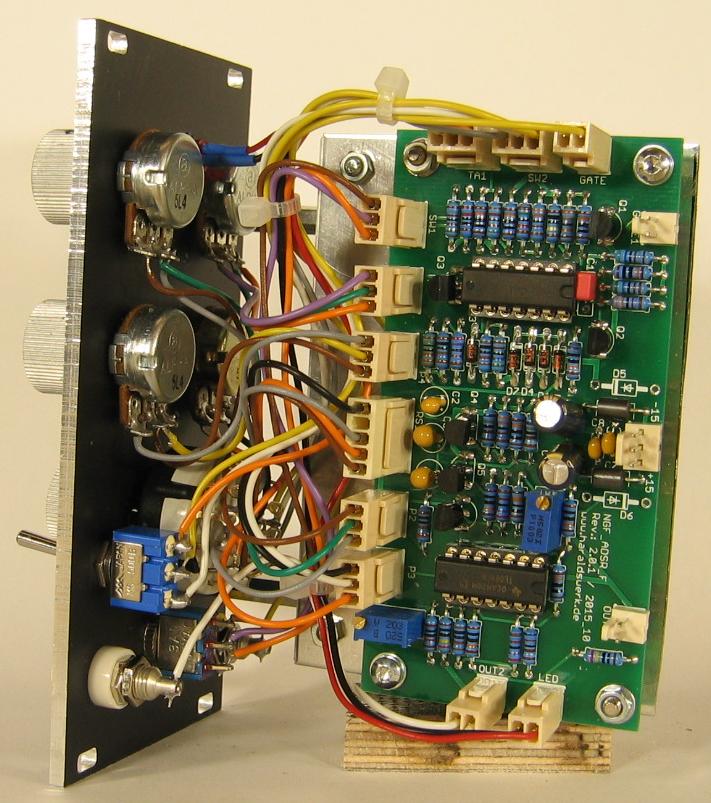
NGF-E Project: ADSR back