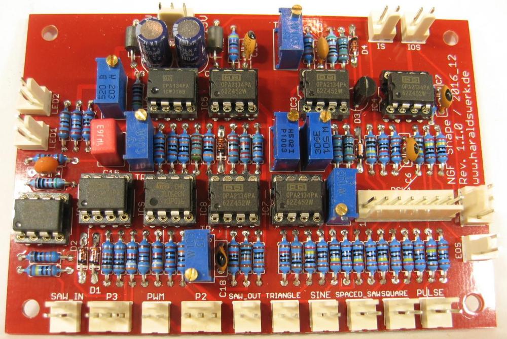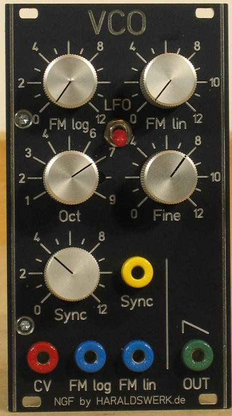
NGF VCO core two faceplate
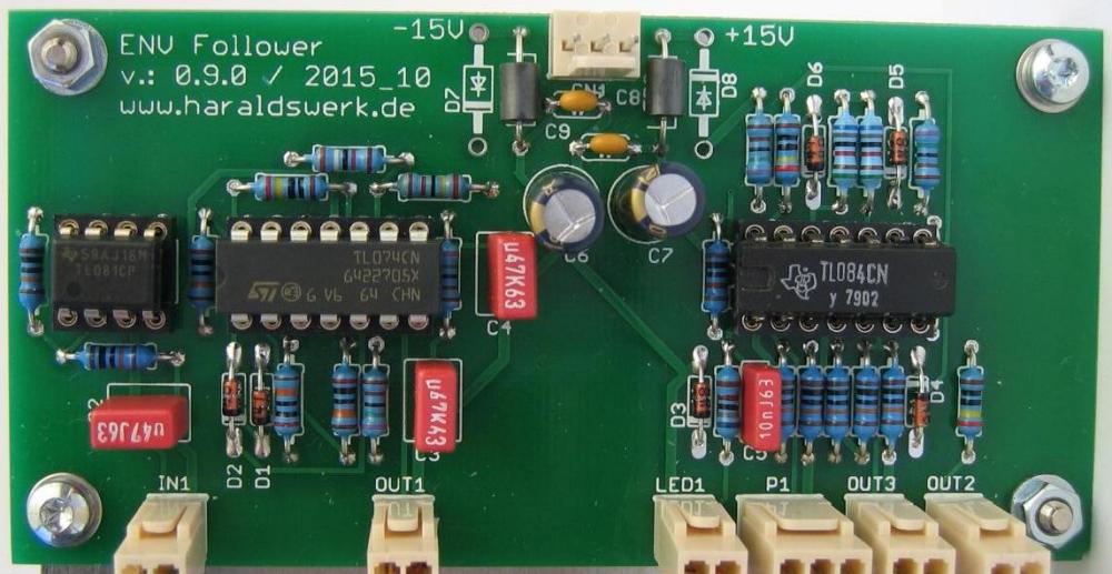
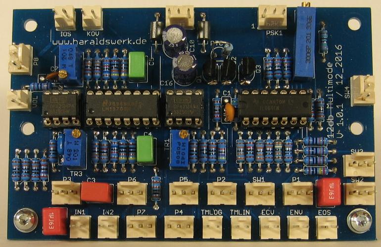
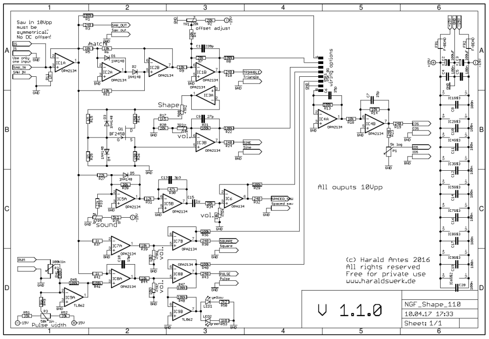
I have build my first original Elektor Formant VCO’s in the 70’s. They worked quite well and do so until today. Over the years i did implement some changes and extensions. I have developed a PCB Version with my changes and extensions published as VCO Core one. But only for those few lucky ones with some spare uA726. Here is the second VCO for my Next Generation Formant project. As in the NGF VCO core one I tried to keep the basic architecture of the original Elektor Formant. With the goal using only today available parts. This means finding a heated transistor pair for the expo converter and a Schmitt Trigger with hysteresis for the switching. Because there are no heated transistor pairs obtainable in the market today I was on my own. There are some solutions for a heated expo pair out there. Most of them build around no longer available parts or quite expensive. A still easy to get and cheap part is the LM3046. The SMD version is still in production today (2017 March) and the DIL version is easy to source as well. Though not longer in production. The PCB for the NGF VCO core two holds both versions. You can stuff it with the SMD- or DIL version. The 4093 is used as Schmitt Trigger for switching. Using the 4093 makes some level shifting necessary for proper switching. The switching capacitor is reduced to 470pF which give an even more better volt per octave characteristic then the original over the audio range. A LFO option is implemented as well. In conjunction with the waveshaper you have now the same waveforms available as voltage controlled LFO.The uA726 is replaced with LM3046 and the 7413 with 4093. All internal control voltages are stabilized. I removed the need for the +5V current supply, added an octave switch, FM lin and sync in. A new feature is the LFO switch. The signal level is raised to 10Vpp to get a better SNR throughout the system.
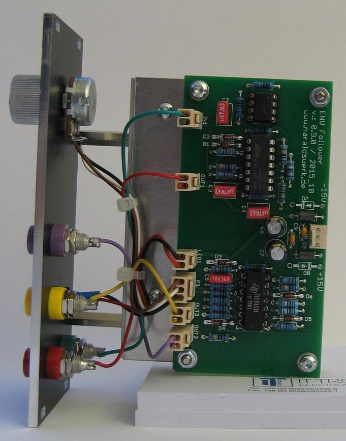
The documentation is available for download on my website.
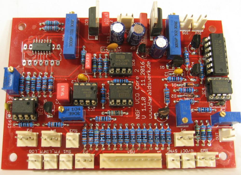
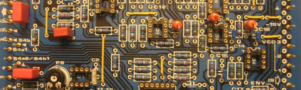
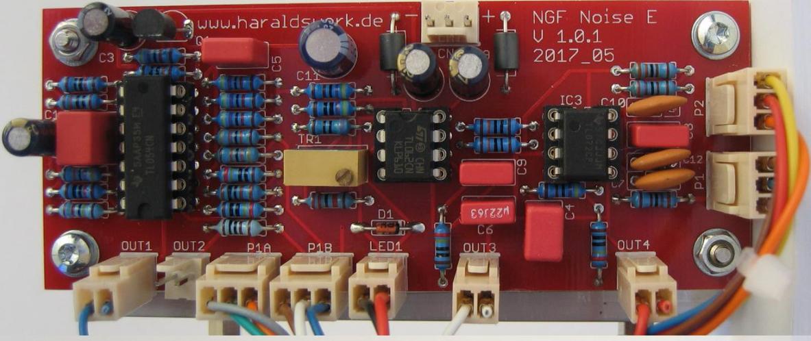
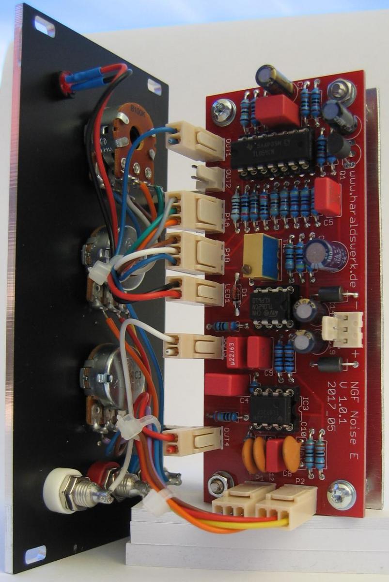
VCO Core two: stuffed PCB
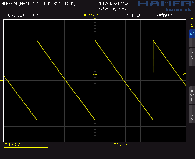
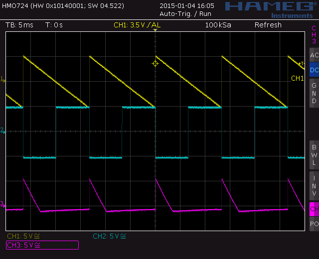
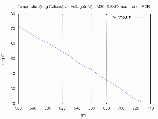
VCO core two saw out
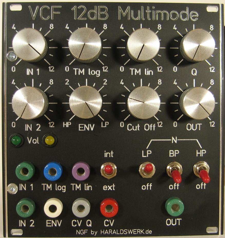
All changes I have made to my original Elektor Formant VCO are implemented: No extra 5V source is needed, all control voltages are stabilized, Octave switch, FM lin, 10Vpp output. New LFO option.
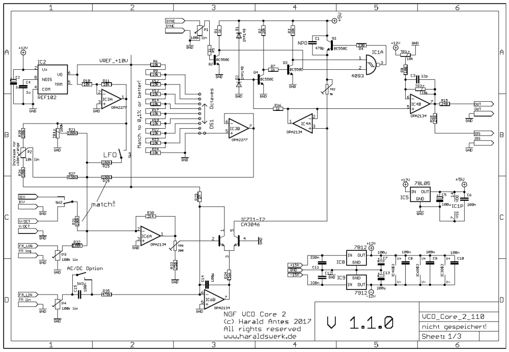
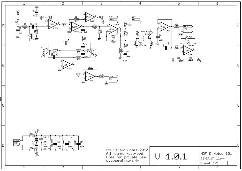
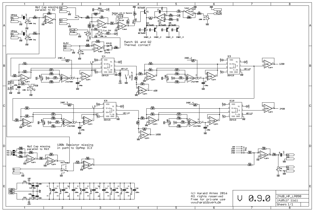
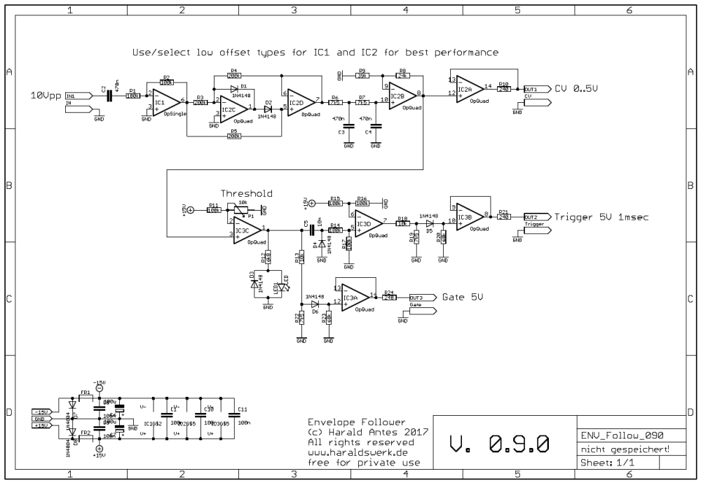
NGF VCO core two schematic
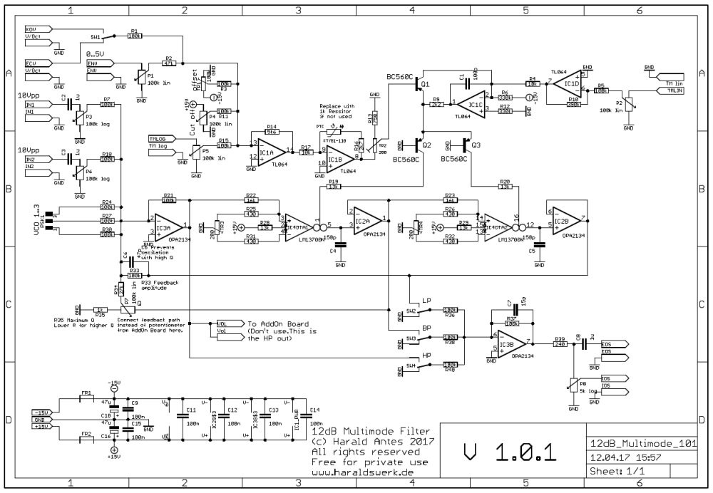
To keep the characteristic of the original Elektor Formant I kept the heated exponential converter, here build around the LM3046. The PCB is developed to hold the DIL and the SOIC version as well. The Schmitt Trigger used is the 4093. Due to different switching levels in the original some transistors are added for level shifting. The octave switch is build with the OPA2277 and the voltage reference REF102. Switch SW1 turns the LFO option on and off. The level for the Sync input is adjusted with P1. Fine tune of the pitch is done with P2. If you need a wider range for the tuning you can change it with changing the potentiometer or the resistors values here. The basic pitch is set with TR4. Output voltage is set with TR3 and the DC offset with TR1.
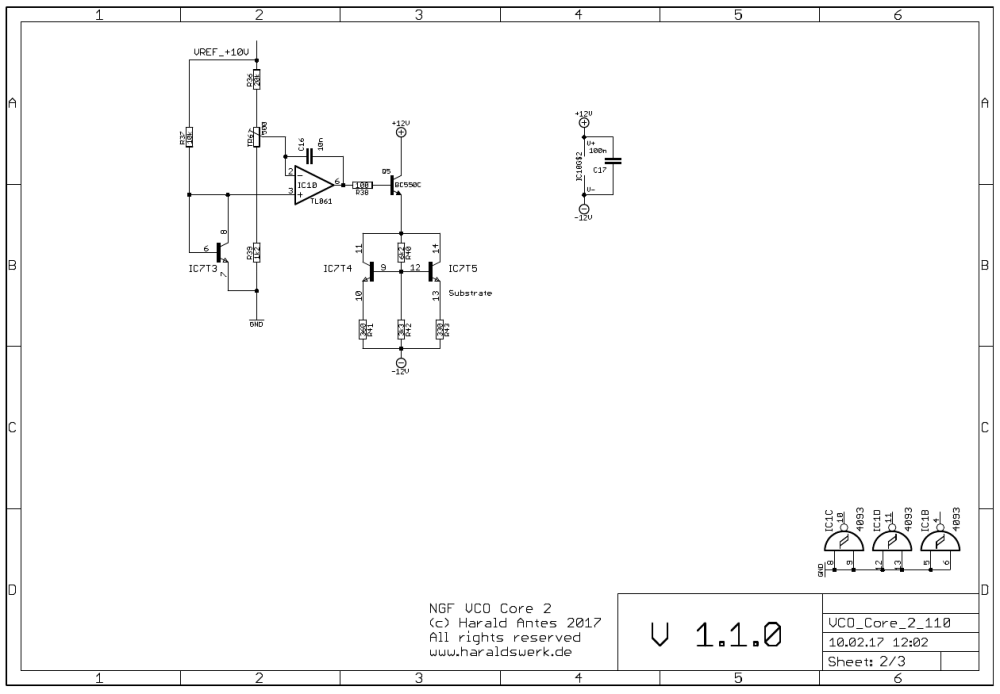
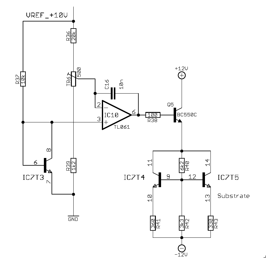
NGF VCO core two schematic heater
This circuitry is part of my NGF VCO Core 2. It make use of two transistors to heat the LM3046. It works with the SMD and DIL Version as well. The given resistor values keep the current values and the power dissipation below the maximum ratings. T3 is used to measure the actual temperature. The voltage drop over T3 is direct proportional to the chip temperature. It is compared to the voltage at pin 2 of the LM3046 which is derived from TR6. The temperature is easily adjusted with TR6. Between heating off and maximum temperature. The testing bridge is driven with a stabilized 10V voltage source. T4 and T5 are used as heaters. R41 and R43 limit the maximum current. The different values are selected with purpose to keep pin 13 of the LM3046 (the substrate) the lowest negative point at the chip.