NGF Project: 440CPS

NGF-E Project: 440CPS front view

NGF-E Project: 440CPS front view

Not much to say. A 440CPS module. Quite useful for tuning in a bigger system. OK, one more sentence. It is the replacement for the 440CPS module from the Elektor Formant in my Next Generation Formant project Project.

Specs and features
• On/Off Switch to keep the 440Hz out of the system when not needed
• Runs on +/-15V and +/-12V
• Power consumption below 25mA +rail / 5mA -rail

The documentation for download can be found in my website.

NGF-E Project: 440CPS schematic

NGF-E Project: 440CPS schematic

Everything is done in software. Output is a 440Hz Square wave. That’s it.

NGF-E Project: 440CPS populated PCB

NGF-E Project: 440CPS populated PCB

NGF-E Project: 440CPS back view

NGF-E Project: 440CPS back view

Limiter / Compresssor

Limiter / Compressor front view

Limiter / Compressor front view

To handle the great dynamic range of the Shakuhachi I needed a compressor for my Shakuhachi 2 Synth project. Because a limiter is not that different I added this feature as well. This comes in handy with my Vocoder project also. The structure used here is derived from “Small Signal Audio Design” by Douglas Self p682ff. The audio signal did not flow through a VCA as in many other implementations. Instead the compression or limitation is done by subtracting the audio signal at the output summing node according to the control voltage derived from the audio signal.

Specs and features
• Switch compress or limit
• Switch Compression/Limit rate 50% or 90%
• Compression/Limit rate adjustable 0–max
• Runs on +/-15V and +/-12V (with minor resistor changes)
• Power consumption below 15mA each rail

The documentation for download can be found in my website.

Limiter / Compressor schematic 01

Limiter / Compressor schematic 01

The audio signal flows unaffected through IC1A/B. When the compressor – limiter kicks in the inverted signal is added (=subtracted) at the summing node of IC1A. The signal level to subtract is regulated through a Sims VCA. The CV generation for the VCA is pretty standard. Linear for the compressor and exponential for the limiter.

Limiter / Compressor schematic 02

Limiter / Compressor schematic 02

Precision full wave rectifier with filter to generate the control voltage for the VCA from the audio signal.

Limiter / Compressor populated PCB

Limiter / Compressor populated PCB

Limiter / Compressor back view

Limiter / Compressor back view

NGF-Project: Elektor Wave Processor

NGF Project: Elektor Wave Processor

NGF Project: Elektor Wave Processor

A small but very versatile module. It is derived from the original Elektor Formant book “Formant Erweiterungen” p87 ff. Some resistor values are changed to handle the 10Vpp signal level of my system. You can shape the input signal in many ways. You can clip the signal. You can fold the signal. You can emphasize the third harmonic. You can unsymmetrical emphasize the clipped and unclipped signal. You can reverse the input signal. The clipping level is voltage controlled.

Specs and features

• Clipping the signal
• Folding the signal
• Emphasize the third harmonic
• Unsymmetrical emphasize the clipped and unclipped signal
• Clipping level voltage controlled
• 10Vpp input and output
• Runs on +/-15V and +/-12V

The documentation for download can be found in my website.

NGF Project: Elektor Wave Processor, schematic

NGF Project: Elektor Wave Processor, schematic

This implementation follows closely the original Elektor Formant implementation. Refer to the original documentation if needed. You can find it on the net. My changes are the adaption to my 10Vpp system signal level.

NGF Project: Elektor Wave Processor, populated PCB

NGF Project: Elektor Wave Processor, populated PCB

NGF Project: Elektor Wave Processor, rear view

NGF Project: Elektor Wave Processor, rear view

NGF Project: Dual Ringmodulator

NGF Project: Dual Ringmodulator front view

NGF Project: Dual Ringmodulator front view

I was a bit hesitant doing this module because it uses the now obsolete LM1496 balanced modulator-demodulator. But you can still source them and I have some in my stock. So I decided to make a PCB and module for my Next Generation Formant project. I started with the original Elektor Formant schematic published in “Formant Erweiterungen” p35ff. I left out the microphone and envelope follower part because I already have such modules. I have added input buffers and raised the signal level to my 10Vpp used throughout my system. I was able to put two ringmodulator on a 50x100mm PCB.

Specs and features
• Dual ringmodulator
• 10Vpp input and output
• Runs on +/-15V and +/-12V

The documentation for download can be found in my website.

NGF Project: Dual Ringmodulator schematic

NGF Project: Dual Ringmodulator schematic

This implementation follows closely the original Elektor Formant implementation. Refer to the original documentation if needed. You can find it on the net. My changes are the input buffers and the adaption to my 10Vpp signal level.

NGF Project: Dual Ringmodulator populated PCB

NGF Project: Dual Ringmodulator populated PCB

NGF Project: Dual Ringmodulator back view

NGF Project: Dual Ringmodulator back view

NGF Vocoder Project: Voiced – unvoiced detection

NGF Vocoder : Voiced - unvoiced detection PCB

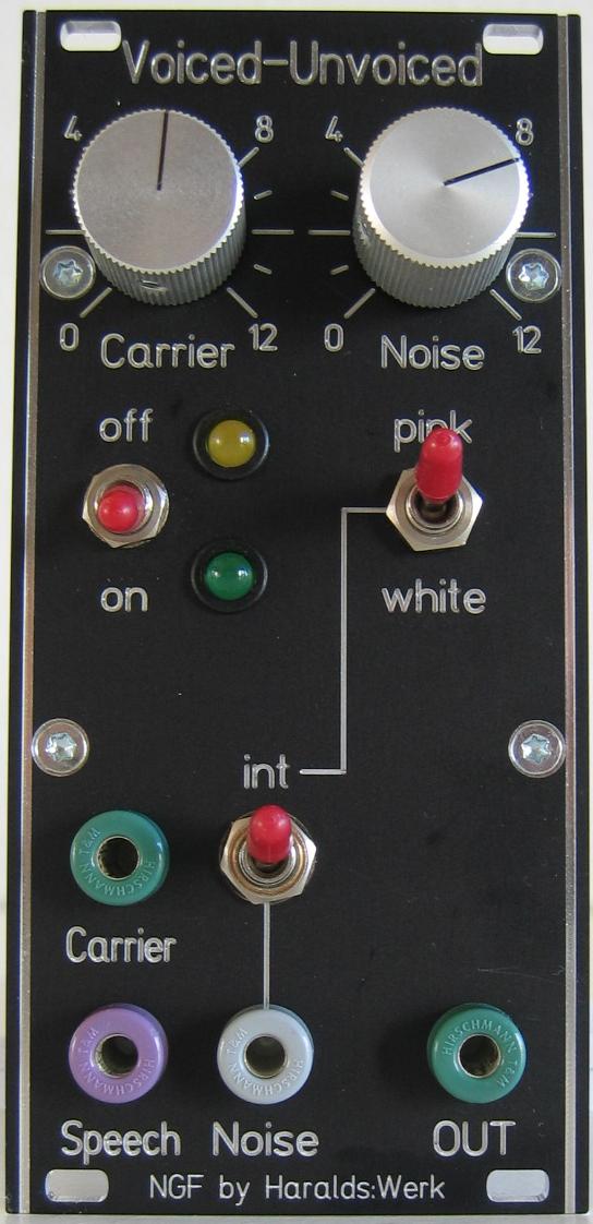
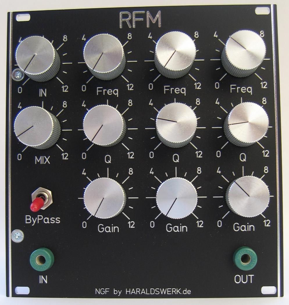
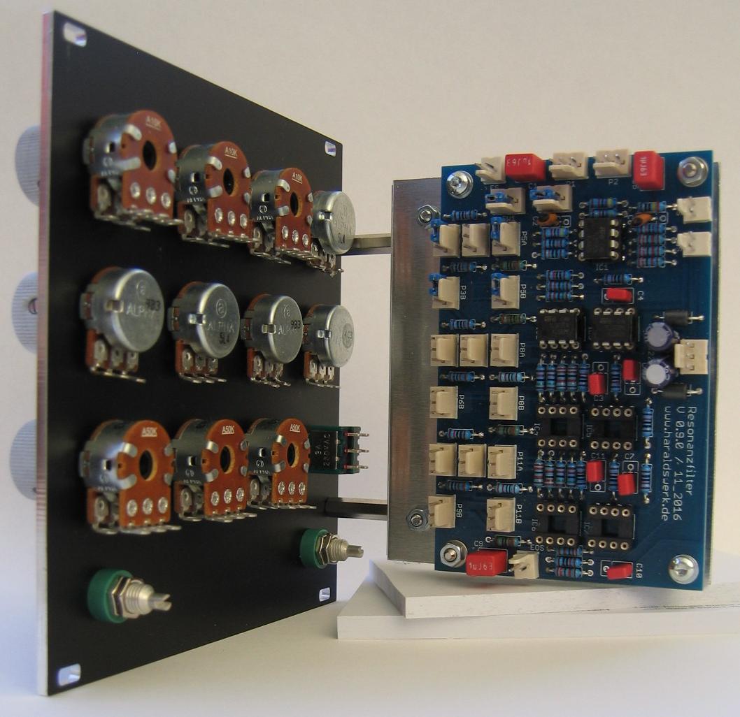
NGF Vocoder : Voiced – unvoiced detection PCB

Here is the voiced – unvoiced detection module for my Vocoder project. It is made off a high pass and a low pass filter. The outputs of the filters are compared. The comparator switches the output signal between carrier and noise.

The documentation for download can be found in my website.

NGF Vocoder project: Voiced - unvoiced detection schematic 01

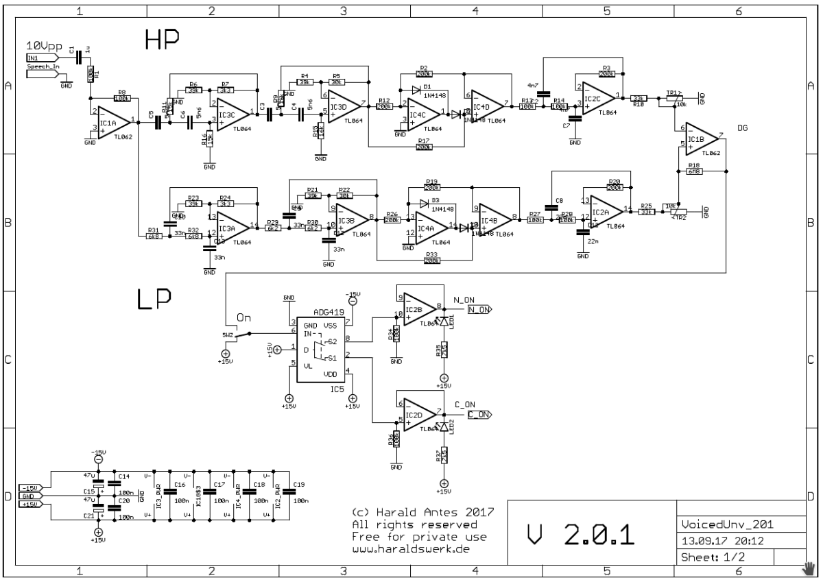
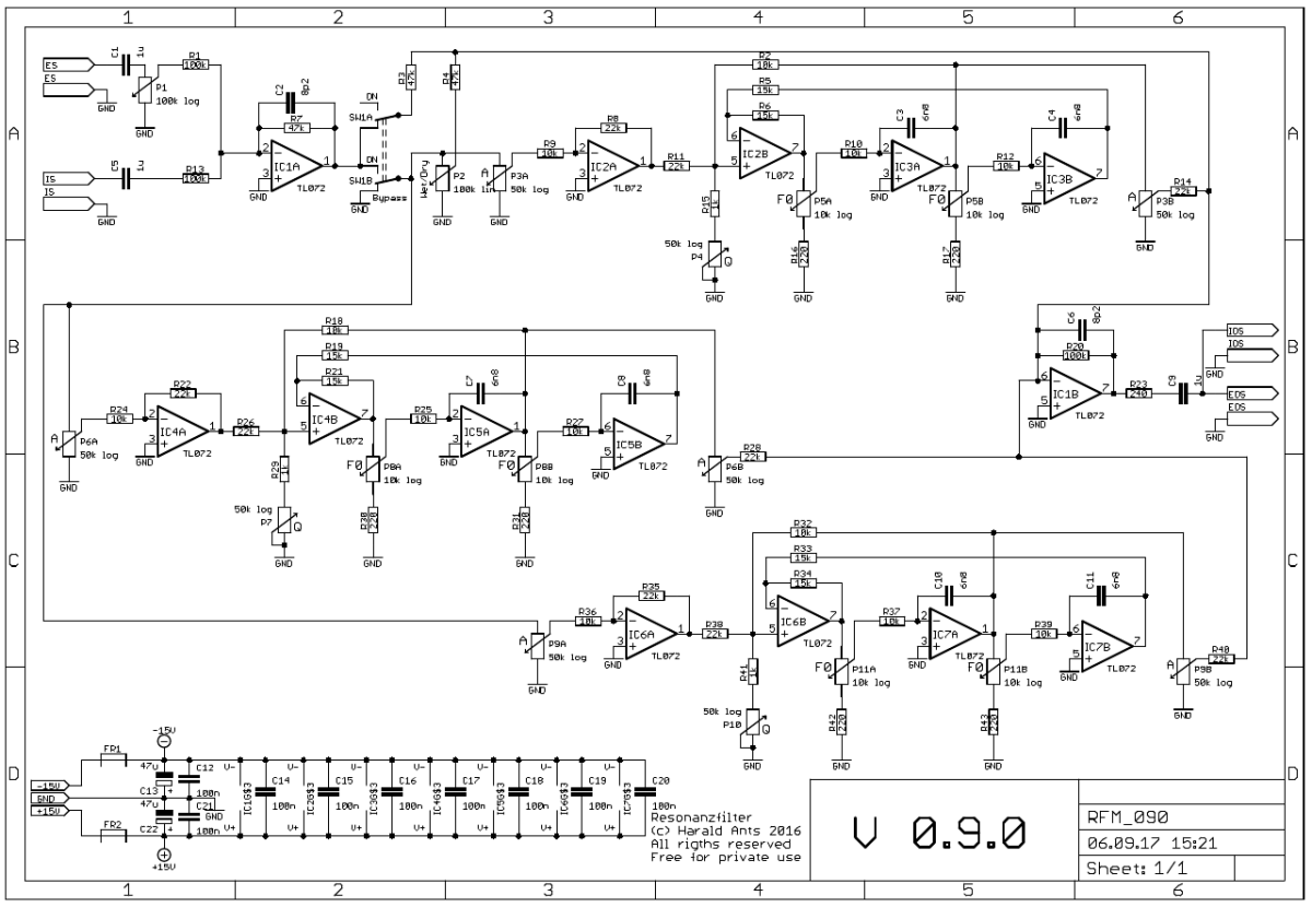
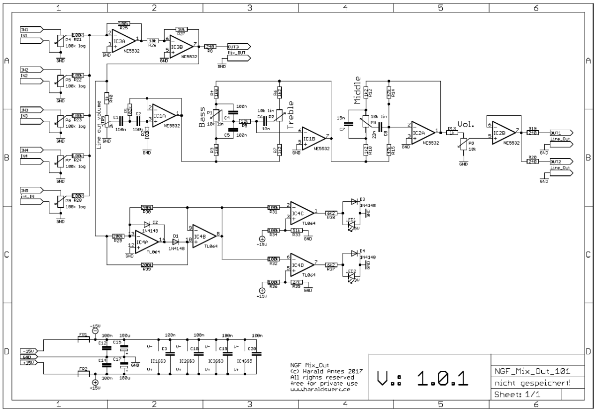
NGF Vocoder project: Voiced – unvoiced detection schematic 01

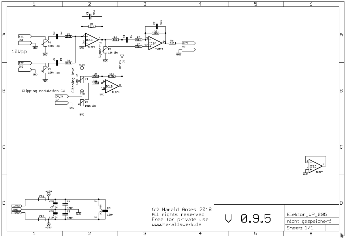
The speech input signal derived from the speech input module initially reaches the buffer IC1A and is then split into two signals, each passing a filter. The high pass filter is constructed around IC3C and IC3D and the low pass around IC3A and IC3B. Their peak values are at 2500Hz and 600Hz respectively. The high pass filter is a Sallen Key filter, highly damped, gain around 5.6 dB. The low pass filter is constructed accordingly. Both filter sections have a slope of 24dB per octave to obtain a good separation. They are each followed by a precision full wave rectifier (IC4C, IC4D and IC4A, IC4B) and by a 12dB per octave smoothing filter. The rectified and calibrated filter output signals are now feed to a comparator IC1B. The voiced – unvoiced decision is taken by the comparator according to the signal levels. The comparator output steers the switch IC5 which selects if the carrier or the noise signal is send to the output.

NGF Vocoder project: Voiced - unvoiced detection schematic 02

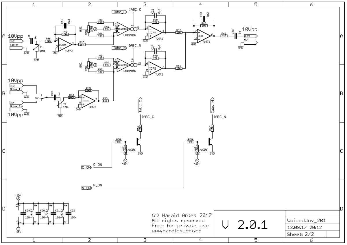
NGF Vocoder project: Voiced – unvoiced detection schematic 02

The carrier and the noise input are both fed to OTA’s. The carrier input is buffered with IC9A, the noise input with IC9B. The noise input is switchable between internal and external source. The OTA’s are turned on or off according to the signal from switch IC5 (schematic page 01).

NGF-E Project: RFM

NGF-E Project: RFM stuffed PCB

NGF-E Project: RFM stuffed PCB

This is my replacement of the original Elektor Formant RFM module. It follows closely the original. Because this one is for my Next Generation Formant project i started with the original Elektor Formant RFM schematic and added my changes to the design. All parts are updated to today (2017/10) available parts. The connections are the same as in the original to keep the possibility for internal wiring. If you don’t need those features just leave them out. This PCB provides all functions as in the original Elektor Formant RFM. The only change I have made is adding a wet/dry potentiometer. So you can adjust the balance between the input signal and the filtered signal

The documentation for download can be found in my website.

NGF-E Project: RFM schematic

NGF-E Project: RFM schematic

The schematic follows closely the original Elektor Formant RFM. For details refer to the original documentation.

NGF-E Project: RFM faceplate

NGF-E Project: RFM faceplate

NGF-E Project: RFM back view

NGF-E Project: RFM back view

NGF-E Project: Mix Out (COM)

NGF-E Project: Mix Out (COM) stuffed PCB

NGF-E Project: Mix Out (COM) stuffed PCB

This is my replacement of the original Elektor Formant COM module used in my Next Generation Formant project. I discarded the original circuitry because of the TL085 used with his unusual pinout and the availability of dedicated audio operational amplifiers. I used a more effective filter implementation for tone control. A mixer front end with four external inputs is added to make patching easier. A optional level indicator makes it easier to find the right volume level for best SNR. The maximum output volume is adjustable to protect your PA

The documentation for download can be found in my website.

NGF-E Project: Mix Out (COM) schematic

NGF-E Project: Mix Out (COM) schematic

Nothing special in this schematic. The tone control is a Baxandall type.
Calibration procedure and more information on my website.

NGF-E Project: Mix Out (COM) front view

NGF-E Project: Mix Out (COM) front view

NGF-E Project: Mix Out (COM) back view

NGF-E Project: Mix Out (COM) back view

NGF-E Project: ADSR

NGF-E Project: ADSR stuffed PCB

NGF-E Project: ADSR stuffed PCB

This is my take on the ADSR. Because this one is for my Next Generation Formant project i started with the original Elektor Formant ADSR schematic and added my changes to the design. All parts are updated to today (2017/09) available parts. The connections are the same as in the original to keep the possibility for internal wiring. If you don’t need those features just leave them out. This PCB provides all functions as in the original Elektor Formant ADSR. I have made a few changes to fix some shortcomings of the original. A triple range switch was added for finer adjustment of the ADSR CV-output signal. The attack rise time is shorter now as in the original. The gate input is buffered. The fixes a fault in the original when working with analog sequencers. The output voltage is slightly raised to reach really 5V. Due to the design of the original Elektor Formant ADSR the output of the original ADSR keeps a residual voltage of about 0,5V. I have put an adjustable compensation in my design to correct this and keep the original behavior if needed as well.

The documentation for download can be found in my website.

NGF-E Project: ADSR schematic

NGF-E Project: ADSR schematic

This is a close clone of the Elektor Formant ADSR. Here i only describe the changes i have made. The description of the other parts of the circuitry can be found in the original Elektor Formant documentation. The gate signal input resistance is raised from 33kOhm to 1megOhm with the input buffer IC1A. This protects against double triggering with the falling edge of the gate signal when using sequencers. R12 is used to fix the input to a defined potential when no signal is attached to the input. R33 and R36 in combination with a push button give you the single shot feature. C1 was lowered to 6n8 from 10nF. In combination with C2 and the raised charging voltage through IC1B/R9 this makes for faster attack time. The load capacitor of 10u was replaced with three selectable capacitors of 2,2uF 4,7uF and 10uF. This make for a finer adjustment of the response times of the ADSR. The voltage divider R24/R25 was adjusted to ensure that the output level of 5V is reached when the offset option with TR2 is used. If this feature is not used R25 should be lowered to 5k1. Construction conditioned the output at IC1D only reaches a minimal voltage of about 0,5V. To compensate for this i added IC2C. With TR2 you can trim the output down to zero volts. If the ADSR is not used the output voltage is now at -0,5V. If you don’t want to use this feature just turn TR2 to ground and you will have the original behavior of the original Elektor Formant ADSR. The current consumption was lowered with using the TL064 and a low current led.
Calibration procedure and more information on my website.

NGF-E Project: ADSR faceplate

NGF-E Project: ADSR faceplate

NGF-E Project: ADSR back

NGF-E Project: ADSR back

NGF-E Project: VCA

NGF-E Project: VCA stuffed PCB

NGF-E Project: VCA stuffed PCB

This is my take on the VCA. Because this one is for my Next Generation Formant project i started with the original Elektor Formant VCA schematic and added my changes to the design. All parts are updated to today (2017/08) available parts. The connections are the same as in the original to keep the possibility for internal wiring. If you don’t need those features just leave them out. This PCB provides all functions as in the original Elektor Formant VCA. The CA3080 are replaced with LM13700. The signal level is raised to 10Vpp for a better signal to noise ratio. The added volume indicator us useful for finding the appropriate signal level. The volume indicator is optional. You can leave it out with no problems for the other functions.

The documentation for download can be found in my website.

NGF-E Project: VCA schematic

NGF-E Project: VCA schematic

This is a close clone of the Elektor Formant VCA. It consists off two OTA’s in serial configuration. The first OTA provides the log response and the second one the linear response. IC2A sums up the external and internal audio signal. The circuitry around IC1A provides the log converter, IC1B the linear current source for the second OTA.
Calibration procedure and more information on my website.

NGF-E Project: VCA front view

NGF-E Project: VCA front view

NGF-E Project: VCA back view

NGF-E Project: VCA back view