Utility Mixer I

Utility Mixer I
Utility Mixer I

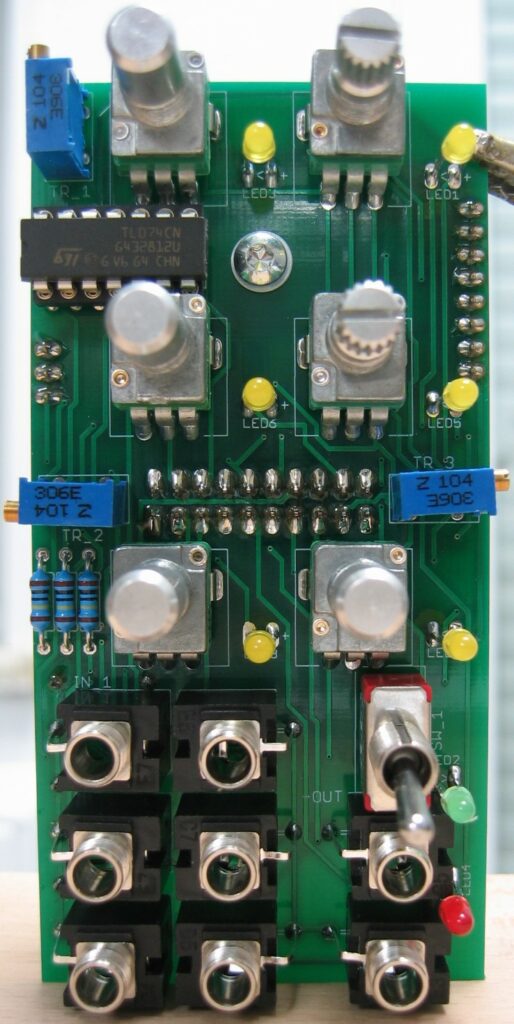
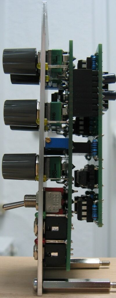
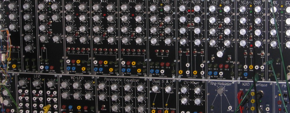
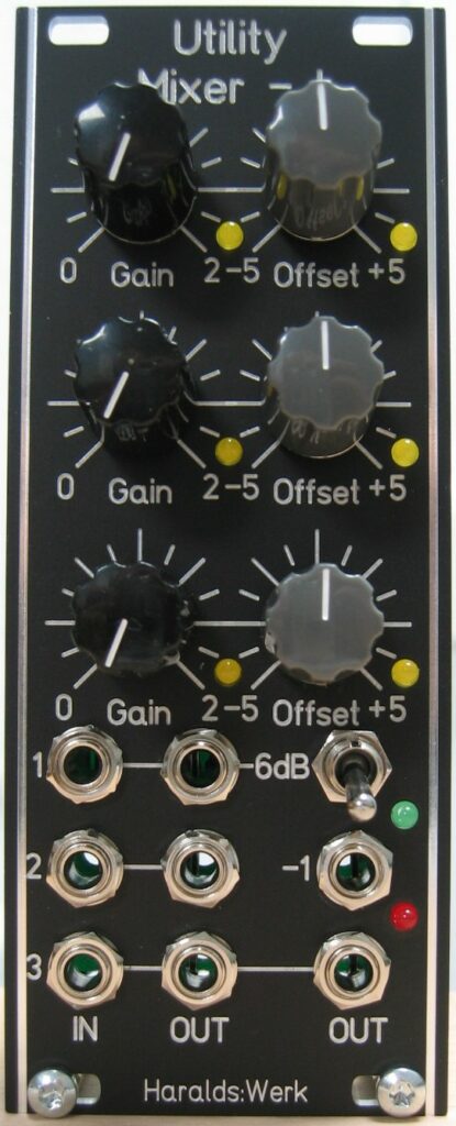
This is an often used utility module. The mixer comes in handy for mixing CV sources. The mixer is DC coupled, so you can use it for DC and AC mixing. The input impedance is constant 1MOhm. The input signals are amplified by a maximum factor of two. It is possible to offset every input with +/- 5V. The offset is signaled with LED’s for every channel and for the summing output. The outputs are normalized, so you can remove selected channels from the output mix. The summed output has a -6dB switchable attenuator. There is an inverted summed output added as well. The added volume indicator us useful for finding the appropriate signal level.

Specs and features

  • Three inputs, three outputs
  • Inverted and non- inverted summed output
  • 2x amplification
  • +/- 5V offset for every channel
  • -6dB switch
  • Volume indicator
  • Normalized outputs
  • Runs on +/-12V and +/-15V
  • Power consumption below 20mA each rail

The documentation and the Gerber files for download can be found in my website.

Utility Mixer I: Main board
Utility Mixer I: Control board

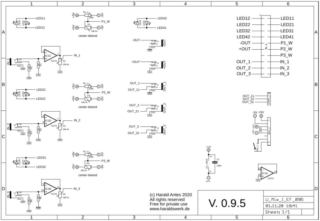
Control board: Straight forward design. The mixer is completely DC coupled. So you can use it for CV mixing as well as audio mixing. IC1B,C,D buffers the three inputs and and keeps the input impedance constant. P2, P4, P6 sets the amplification from zero to 2X. P1, P3, P5 sets the offset voltage. The LED indicates the offset and signal level.

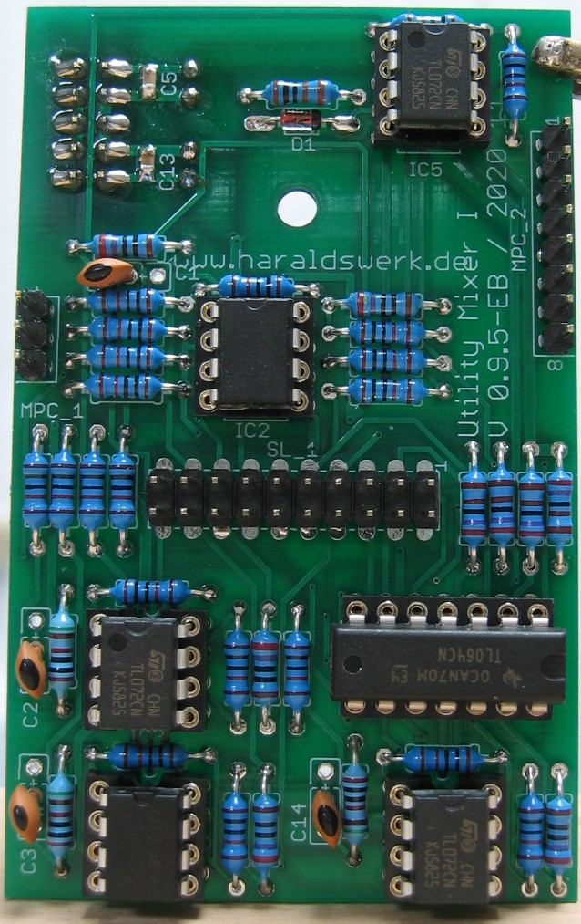
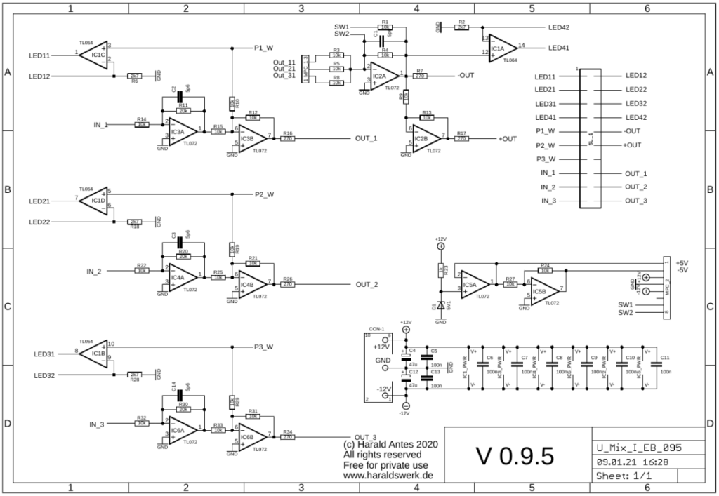
Main board: IC3B, IC4B, IC6B adds the offset voltage and the signal. IC1C, IC1D, IC1B, IC1B drive the low current LED. IC2A sums the signals and drives the negative output. IC2B drives the positive output.

Utility Mixer I: Populated control board
Utility Mixer I: Populated main board
Utility Mixer I: Side view
Utility Mixer I: Back view

ADSR Euro-rack

ADSR: Front view
ADSR: Front view

This is another derivation off the ADSR for my NGF-E project, adapted to 12V Euro-rack format. Because this one is a stand alone module I have removed all additional features from the Next Generation Formant project. Nonetheless it is still based on original Elektor Formant ADSR schematic. I made some error corrections and added my changes to the design. All parts are updated to today (2021/01) available parts. I have made a few changes to fix some shortcomings of the original. A triple range switch was added for finer adjustment of the ADSR CV-output signal. The attack rise time is shorter now as in the original. The gate input is buffered. The fixes a fault in the original when working with analog sequencers. The output voltage is slightly raised to reach really 5V. Due to the design of the original Elektor Formant ADSR the output of the original ADSR keeps a residual voltage of about 0,5V. I have put an compensation in my design to correct this. The driver circuitry for the output indicator LED is changed for better linearity.

Specs and features

  • AD/ADSR switch
  • Gate input 5V
  • CV output ..5V
  • CV output indicator
  • Range switch: fast, middle, long
  • Attack (A) 0,5ms…16s
  • Decay (D) 4ms…40s
  • Sustain (S) 0..5V
  • Release (R) 4ms..40s
  • Power consumption below 15mA each rail

The documentation and the Gerber files for download can be found in my website.

ADSR: Schenmatic main PCB
ADSR: Schematic main PCB
ADSR: Schematic control PCB

This is a close clone of the Elektor Formant ADSR. Here i only describe the changes i have made. The description of the other parts of the circuitry can be found in the original Elektor Formant documentation. The gate signal input resistance is raised from 33kOhm to 1megOhm with the input buffer IC1A. This protects against double triggering with the falling edge of the gate signal when using sequencers. R30 is used to fix the input to a defined potential when no signal is attached to the input. C1 was lowered to 6n8 from 10nF. In combination with C2 and the raised charging voltage through IC1B/R9 this makes for faster attack time. The load capacitor of 10u was replaced with three selectable capacitors of 2,2uF 4,7uF and 10uF. This makes for a finer adjustment of the response times of the ADSR. The voltage divider R19/R21 was adjusted to ensure that the output level of 5V is reached. If this feature is not used R25 should be lowered to 5k1. Construction conditioned the output at IC1D only reaches a minimal voltage of about 0,5V. To compensate for this i added IC2A. If the ADSR is not used the output voltage is now at -0,5V. The current consumption was lowered with using the TL064 and a low current LED.

ADSR: back view
ADSR: Back view
ADSR: Populated main PCB
ADSR: Populated control PCB
ADSR: Side view
ADSR: Side view

Pitch to voltage converter

Pitch to voltage converter: Front view

This is the software driven replacement for my all hardware pitch to voltage converter from my Shakuhachi to Synth project. The software driven approach has the advantage of easily adaption for different frequency ranges. In my case it is the range of the Shakuhachi. To change the range just adapt the software. It is completely temperature independent. The needed input is a pulse train derived from your original signal. You can use my Signal to Trigger converter to provide the pulse train. An offset voltage is added to the V/Oct output to fit the needs of your VCO (Synthesizer).

Specs and features

  • Software driven pitch to voltage converter
  • 12bit resolution
  • V/Oct output
  • Offset CV Fine and coarse adjustment
  • Runs on +/-15V and +/-12V
  • Power consumption around 45mA positive rail, 15mA negative rail

The documentation and the Gerber files for download can be found in my website.

Pitch to voltage converter: Microprocessor board
Pitch to voltage converter: Control board

The incoming pulse train is feed to the microprocessor. IC1 (301-F) prevents the microprocessor from negative inputs. Zener D2 prevents from overvoltage. The trigger starts an internal timer of the microprocessor in input capture interrupt mode. The ticks are counted and the count is then looked up in a table. The lookup table provides the values for the V/Oct conversion. The read value is the send to the DAC MCP4921 which is follwed by a low pass (IC1A, 301-B)). IC2A (301-F) adds the offset voltage and IC2B (301-F) corrects the phase.

Pitch to Voltage converter: Populated PCB's
Pitch to Voltage converter: Populated PCB’s
Pitch to Voltage converter: Side view

Quad white and colored noise source. Quad random voltage source

Quad white and colored noise source. Quad random voltage source. Schematic control PCB
Quad white and colored noise source. Quad random voltage source: Front view

It is quite useful to have different adjustable noise and random voltage sources. Depending on your patch stile of course. Here is the quad version of my noise module from the NGF project. It is a combination of two original Elektor Formant modules. The noise module from Elektor Formant book one and the colored noise (CNC) module from book two. It provides four independent white noise outputs, four adjustable colored noise outputs with “red” and “blue” adjustment. The four random voltage outputs are adjustable in speed of change. The noise is derived from the reverse biased BE diode of an NPN transistor.

Specs and features

  • Four independent white noise outputs
  • Four independent adjustable colored noise outputs with “red” and “blue” adjustment
  • Four random voltage outputs, adjustable in speed of change
  • Four LED indicating the random voltage change
  • Runs on +/-12V and +/-15V
  • Power consumption around 65mA each rail

The documentation and the Gerber files for download can be found in my website.

Quad white and colored noise source. Quad random voltage source. Schematic control PCB
Quad white and colored noise source. Quad random voltage source: Schematic control PCB
Quad white and colored noise source. Quad random voltage source. Schematic main PCB

Description:

(Given for one of the four.) Noise source is the reverse biased BE diode of NPN transistor Q1 (B_090). The following operational amplifier IC1A and IC1B (B_090) amplifies the noise to 10Vpp. IC1C (B_090) is the buffer for the white noise output. IC2B (F_101) is configured as a 12dB low pass. So you get a low frequency random voltage. The changing speed is set with P3A/P3B (F_101) which sets the corner frequency of the low pass filter. IC2A / LED1 (F_101) makes the fluctuation visible. TR_1 (F_101) adjust the brightness of LED1 (F_101). In the feedback loop of IC1B (F_101) is an adjustable filter combination which gives you a wide range of adjustable colored noise with P1 and P2 (F_101). The output is buffered with IC1A (F_101).

Quad white and colored noise source. Quad random voltage source. Populated control PCB
Quad white and colored noise source. Quad random voltage source. Populated main PCB

Scaled voltage reference with octave and semitone steps

Scaled voltage reference with octave and semitone steps. Front view

This module provides high precision CV outputs in 1V (octaves) and 83,3mV (halves) steps. The 1V output goes from -5 to +5V. The 83,3mV steps goes from -5 to plus 5 steps (halves). This module is thought for all who are missing octave switches in some modules. Especially in VCO. With this module you can switch octaves and halves as well.

Specs and features

  • High precision output 0-8V in 1V steps (octaves)
  • High precision output in 83,3mV steps, +/- 5 steps (Halves)
  • Runs on +/-15V and +/-12V
  • Power consumption around 30mA each rail

The documentation and the Gerber files for download can be found in my website.

Scaled voltage reference with octave and semitone steps. Populated PCB
Scaled voltage reference with octave and semitone steps. Schematic

The precision voltage is derived from the REF102. The negative voltage is provided with the INA105. It is crucial to match the resistors in the voltage dividers as good as you can. The outputs of the voltage dividers are buffered to avoid loading of the dividers. The resistors around the OpAmps must be matched as well. The one volt and the 83,3mV steps are added together with IC4A. The three outputs are individual buffered.

Scaled voltage reference with octave and semitone steps. Populated PCB

Voltage controlled quadrature LFO

Voltage controlled quadrature LFO front view
Voltage controlled quadrature LFO

I want to rotate sound through four channels of my modular synthesizer. Or move successive through different CV or audio sources. This is easily achieved with a quadrature LFO and four VCA. The core of this voltage controlled quadrature LFO was published in Electronotes EN#122 pg13ff 1981 and designed by Thomas Henry. I took the core and added the voltage control and the sine shapers.

Specs and features

  • Four triangle quadrature outputs, 90° apart
  • Four sine quadrature outputs, 90° apart
  • Voltage controlled
  • Hi-Low range switch
  • Frequency from 30Hz down to some minutes
  • FM lin
  • FM log
  • Runs on +/-15V and +/-12V
  • Power consumption around 30mA each rail

The documentation and the Gerber files for download can be found in my website.

Voltage controlled quadrature LFO schematic 01
Voltage controlled quadrature LFO populated PCB
Voltage controlled quadrature LFO schematic 02

The voltage control part and the sine shaper are well known designs. The triangle core is commonly used as well. The interesting part is how the 90° triangle is derived. The Electronotes EN#122 gives a very detailed description what is going on.

Voltage controlled quadrature LFO populated PCB
Voltage controlled quadrature LFO triangle output screenshot
Voltage controlled quadrature LFO sine output screenshot
Voltage controlled quadrature LFO back view

Voltage controlled LFO: Flat Version

Voltage controlled LFO front view
Voltage controlled LFO

This is the flat version of my VC-LFO I’ve build this flat version to minimize the depth of the module and avoid the wiring for the potentiometers. A VC LFO with multiple synced output waveforms is a very useful and versatile module. You can’t have enough of them. They can add a lot to sounds making them more animated. This one provides triangle, ramp up, ramp down pulse. square and sine wave output (-5V to +5V). The frequency range is easily adjusted to your needs from some minute per cycle up to 700Hz. I started with the VC LFO design form Ray Wilson MFOS but changed the exponentiator and pulse adjust schematic completely. I have added a range switch and a linear FM input as well.

Specs and features

  • Synced triangle, ramp up, ramp down, pulse, square and sine wave output
  • Output -5V to +5V
  • log and lin CV input
  • Temperature compensated
  • Voltage controlled pulse width
  • Range switch
  • Coarse and fine frequency setting
  • Runs on +/-15V and +/-12V
  • Power consumption below 10mA each rail

The documentation and the Gerber files for downloadcan be found in my website.

Voltage controlled LFO schematic
Voltage controlled LFO schematic back PCB
Voltage controlled LFO schematic
Voltage controlled LFO front PCB

C1 and associated components comprise a linear voltage to log current converter. IC1A sums the control voltages. IC1B provides the temp compensation realized with KTY81-110. TR3 adjusts the V/Oct characteristic. Q1 and Q2 forms the log converter with IC1D as constant current source. IC1C scales the control voltage for the linear FM input. The transconductance of IC1OTA1 controls the frequency of the oscillator. IC2C, C1 and associated components comprise an integrator. When current flows into IC1OTA1 output the integrator ramps up, when current flows out of IC1OTA1 the integrator ramps down. When the integrators output goes above the threshold of comparator IC2D its output goes high. The output of IC2D is fed to the non-inverting input of IC1OTA1 OTA through D1, D2, R1, R2 and TR1. TR1 balances the current flowing during the high and low periods of IC2D. With TR1 you can adjust the symmetry of the triangle. While IC2Ds output is high current flows out of IC1OTA1 OTA and the integrator ramps down until the voltage at the input of IC2D goes low enough to overcome the hysteresis provided by R13 and its output goes low. When this happens the comparator starts to ramp up again and thus we have a triangle wave at the output of IC2C. The bias of the comparator IC2D is controlled by the current generated by the linear voltage to log current convertor. This controls the current that flows in and out of IC1OTA1 and thus the frequency of the oscillator.

The sawtooth is created by mixing portions of the original triangle wave and an inverted version of the triangle wave. N-FETs Q1 and Q1 are used as analog switches.

Voltage controlled LFO screenshot waveforms: ramp up, pulse, square
Voltage controlled LFO screenshot waveforms: ramp, pulse, square
Voltage controlled LFO screenshot waveforms: triangle ramp down, sine
Voltage controlled LFO back view
Voltage controlled LFO side view

12V to 5V gate converter

12V to 5V gate converter schenatic
12V to 5V gate converter front panel

This utility module converts a 12V gate to a 5V gate. It is needed when you have a module with 12V gate output and your receiving module only accepts 5V gate voltage.

Specs and features

  • Converts 12V gate to 5V gate
  • Runs on +/-12V

The documentation and the Gerber files for download can be found in my website.

12V 2 5V gate converter schematic

The 12V input is divided down with the input voltage divider to 5V and buffered.

12V 2 5V gate converter populated PCB
12V 2 5V gate converter side view

CV Mover

CV Mover faceplate

CV Mover faceplate

This utility module provides you with different functions. You can use it as attenuator and sign changer for any input signal. You can use it as CV Source. It gives you a DC offset between -2.5V ans + 2.5V with coarse and fine adjustment. This voltage range is easily adopted to your needs with simple resistor change. Most interesting application is using it as “CV Mover”. This means adding a DC offset to the input signal. Say you have a LFO signal between +/-5V and want to shift it in the positive range. Then you can divide the signal in half with the attenuator to 1/2 and add the +2.5 threshold and you get a 0..5V positive LFO signal. This comes in handy for steering filters VCA’s and other modules. The output signal is visualized with LED

Specs and features
• CV source -2.5..+2.5V with coarse and fine adjustment
• Attenuator
• Positive and inverted output signal
• Adjustable DC offset for the input signal
• Positive and negative CV output indicator with LED
• Runs on +/-15V and +/-12V

The documentation and the Gerber files for download can be found in my website.

CV  Mover: schematic

CV Mover: schematic

IIC1B acts as a simple inverting voltage adder. The input signal and the offset voltages are added together. The direct output from IC1B is the negative of the input signal. IC1A converts the signal back to the original phase. IC1C is a simple buffer and in the feedback loop of IC1D are the indicator LED’s.

CV Mover populated PCB

CV Mover populated PCB

VC LFO

VC LFO front

VC LFO front

A VC LFO with multiple synced output waveforms is a very useful and versatile module. You can’t have enough of them. They can add a lot to sounds making them more animated. This one provides triangle, ramp up, ramp down pulse. square and sine wave output (-5V to +5V). The frequency range is easily adjusted to your needs from some minute per cycle up to 700Hz. I started with the VC LFO design form Ray Wilson MFOS but changed the exponentiator and pulse adjust schematic completely. I have added a range switch and a linear FM input as well.

Specs and features
• Synced triangle, ramp up, ramp down, pulse, square and sine wave output
• Output -5V to +5V
• log and lin CV input
• Voltage controlled pulse width
• Range switch
• Coarse and fine frequency setting
• Runs on +/-15V and +/-12V
• Power consumption below 10mA each rail

The documentation for download can be found in my website.

VC LFO schematic

VC LFO schematic

VC LFO waveforms screenshot

VC LFO waveforms screenshot

VC LFO waveforms screenshot

VC LFO waveforms screenshot

VC LFO populated PCB

VC LFO populated PCB