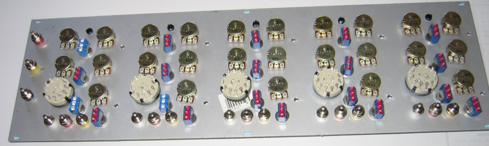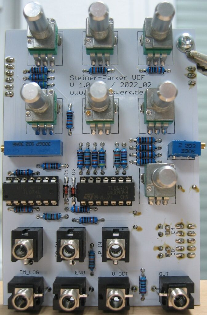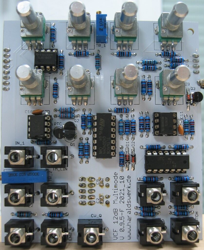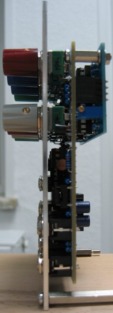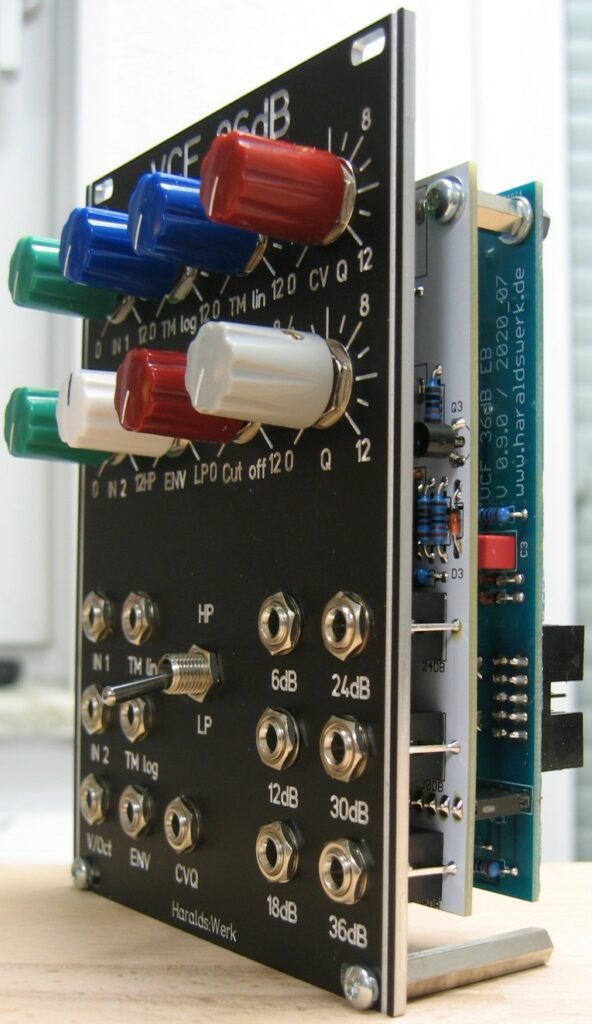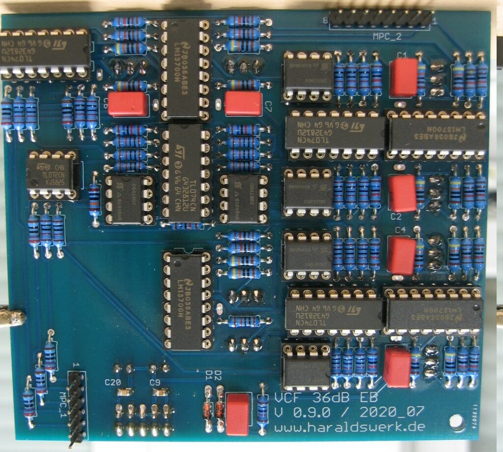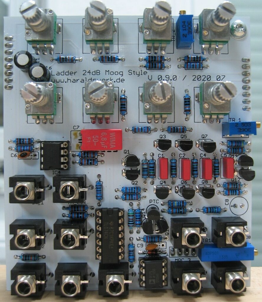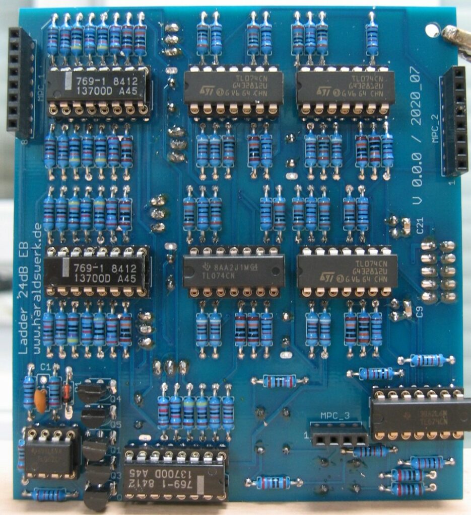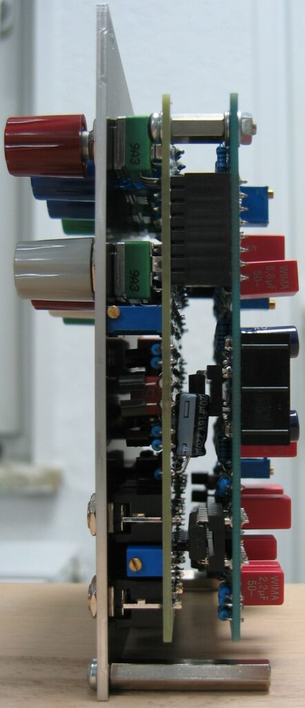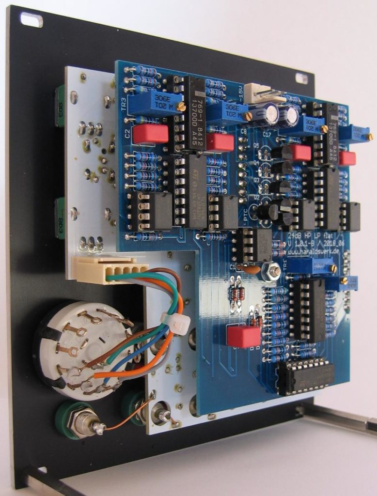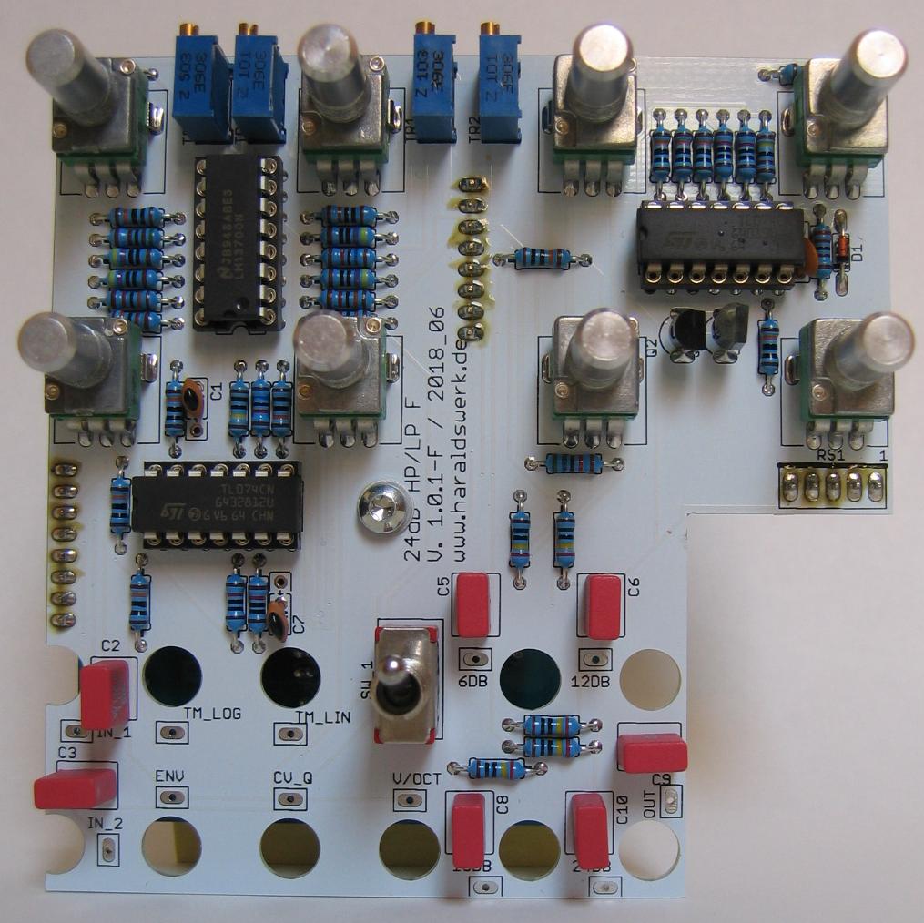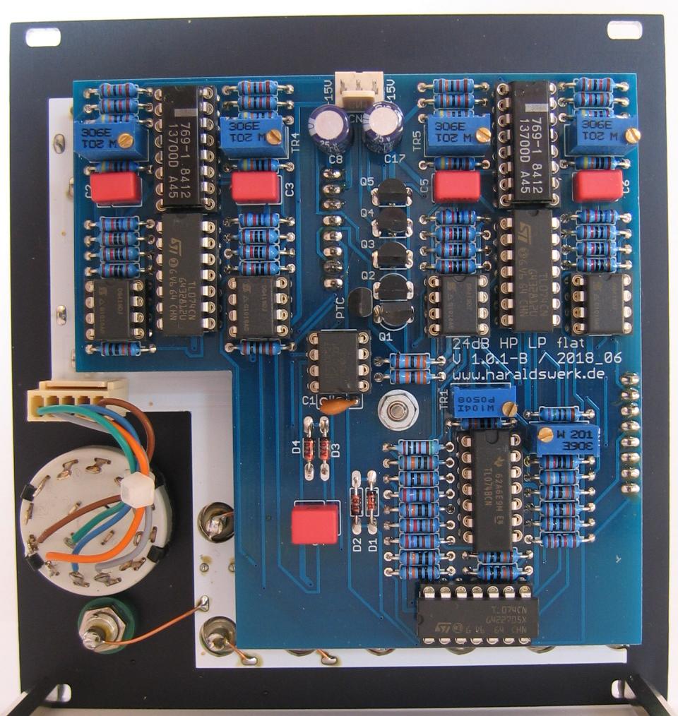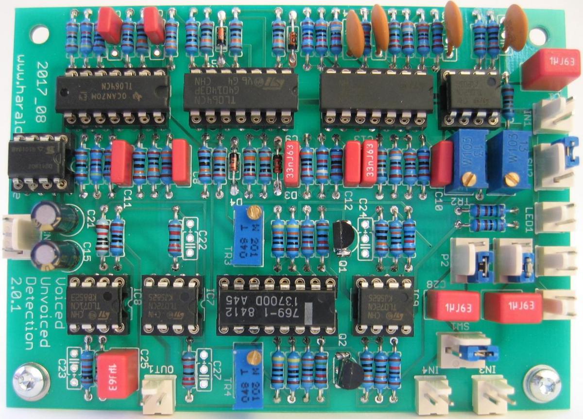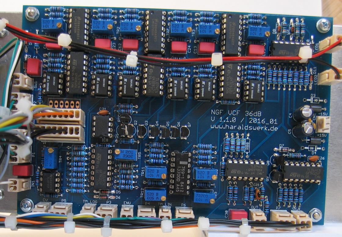
36dB VCF LP/HP populated PCB
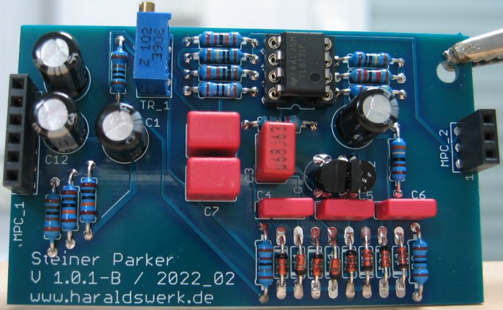
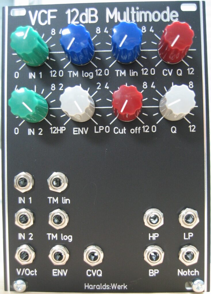
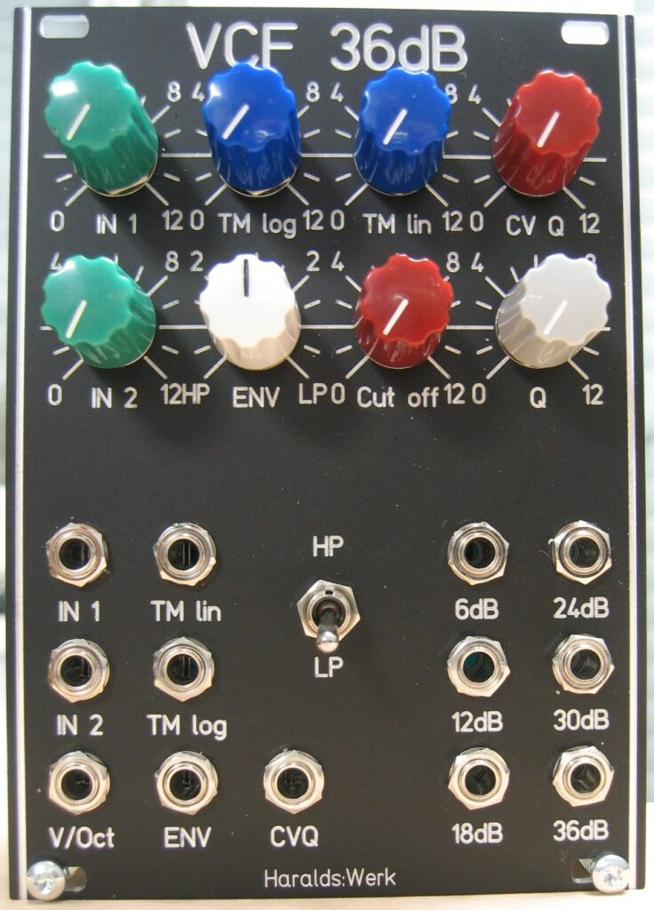
I just wanted to know how a 36dB VCF sounds like. So i build one. This one is basically derived from my 24dB VCF LP/HP which i build for my Next Generation Formant project. I just added two more filter stages and the compensation circuitry from my Moog Ladder filter to compensate for the volume loss when Q is turned up. I have brought out all 6 filter stage outputs. Depending on your wiring you can use a switch to select between the outputs or/and bring all outputs out in parallel. The LP/HP switching is done with electronic switches on the PCB to avoid the problems (hum, noise…) of the wiring with a mechanical switch.
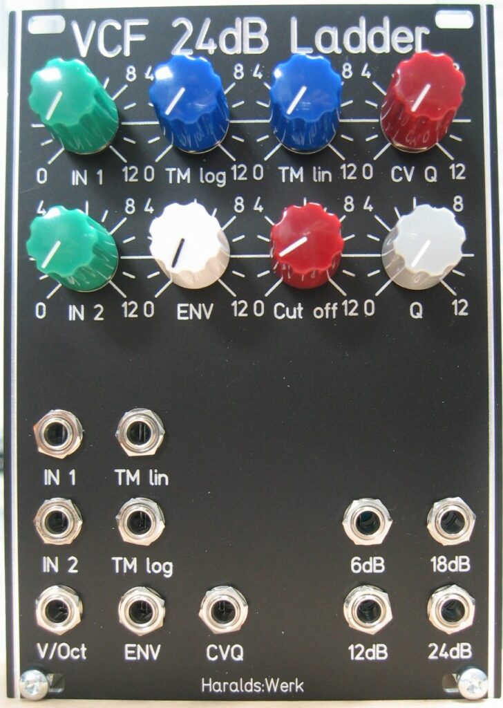
Specs and features
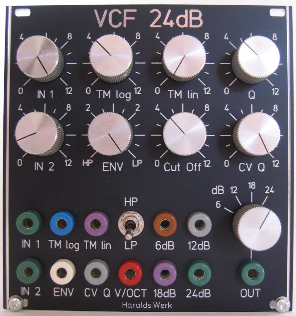
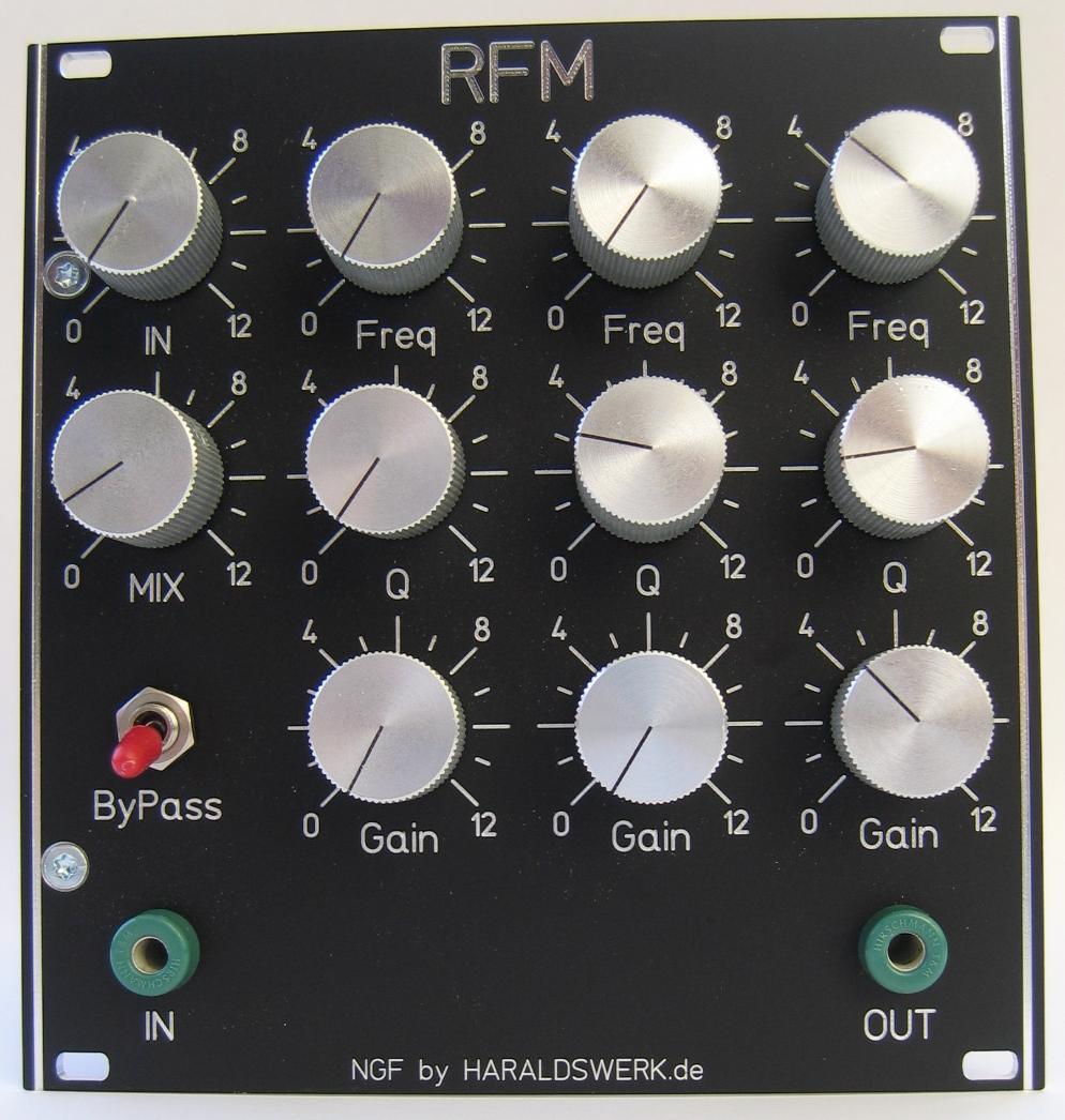
36dB voltage controlled low pass and high pass filter
Switchable output 6dB, 12dB, 18dB, 24dB, 30dB, 36dB
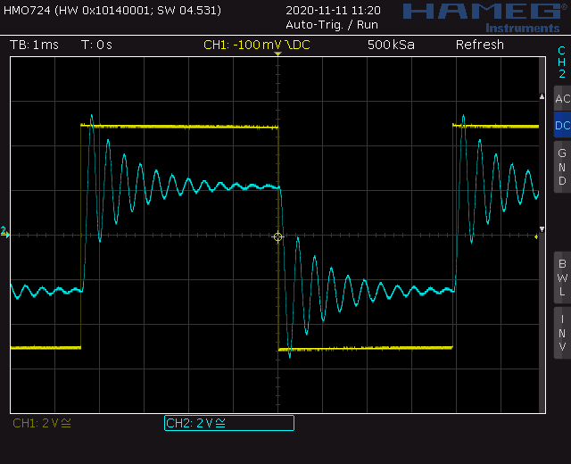
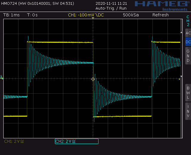
Volume loss compensation with high Q
10Vpp signal level
Voltage controllable Q
Voltage controlled lin and log timbre modulation
Positive and negative ENV control with sign changer
Runs on +/-15V and +/-12V (with minor resistor changes)
Power consumption below mA each rail
Volume indicator (optional)
The documentation for download can be found in my website.
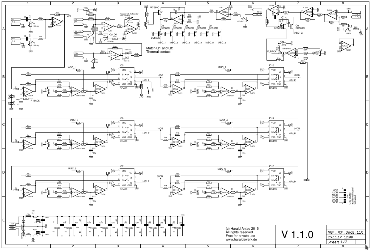
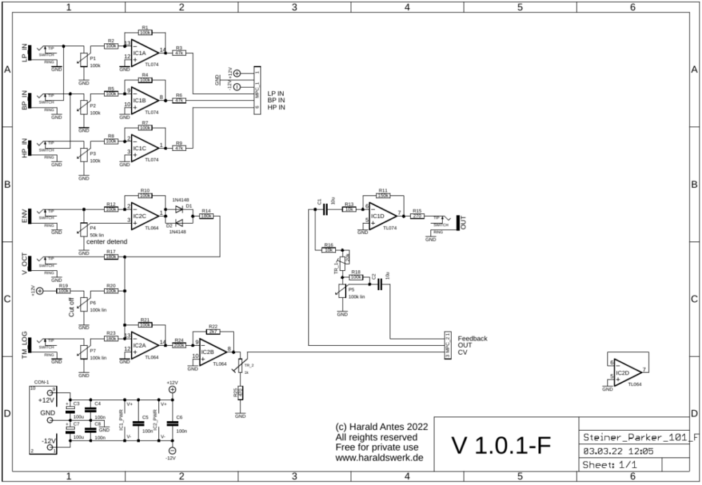
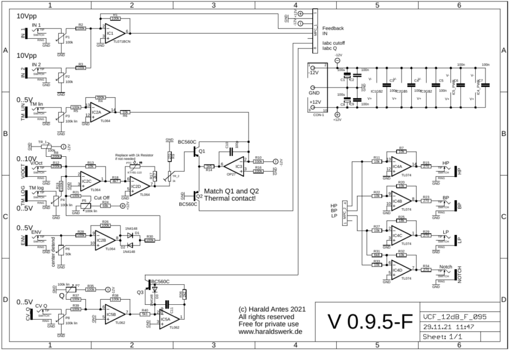
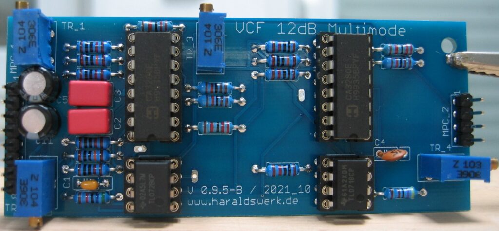
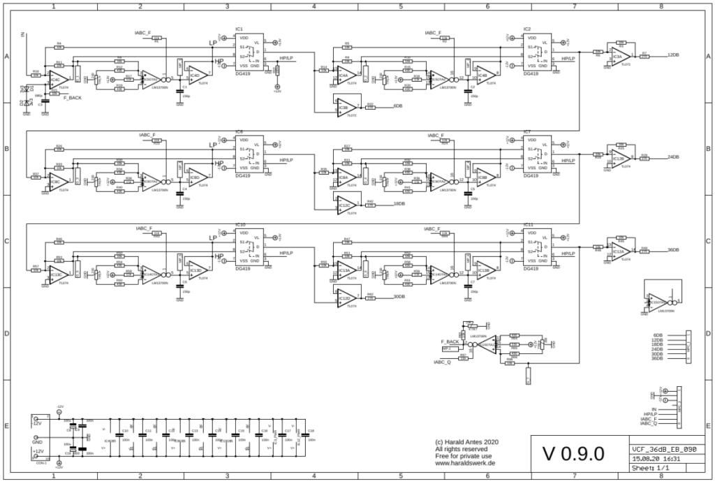
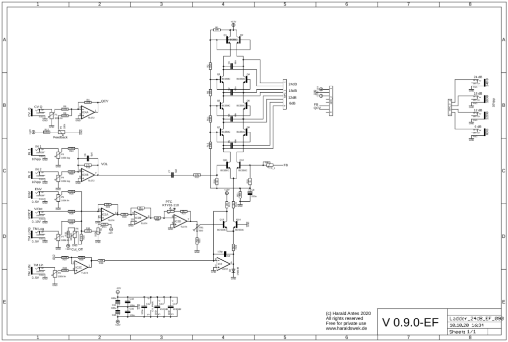
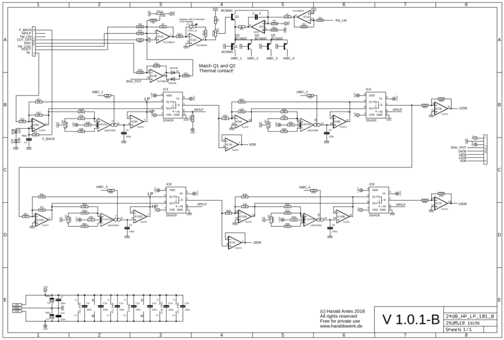
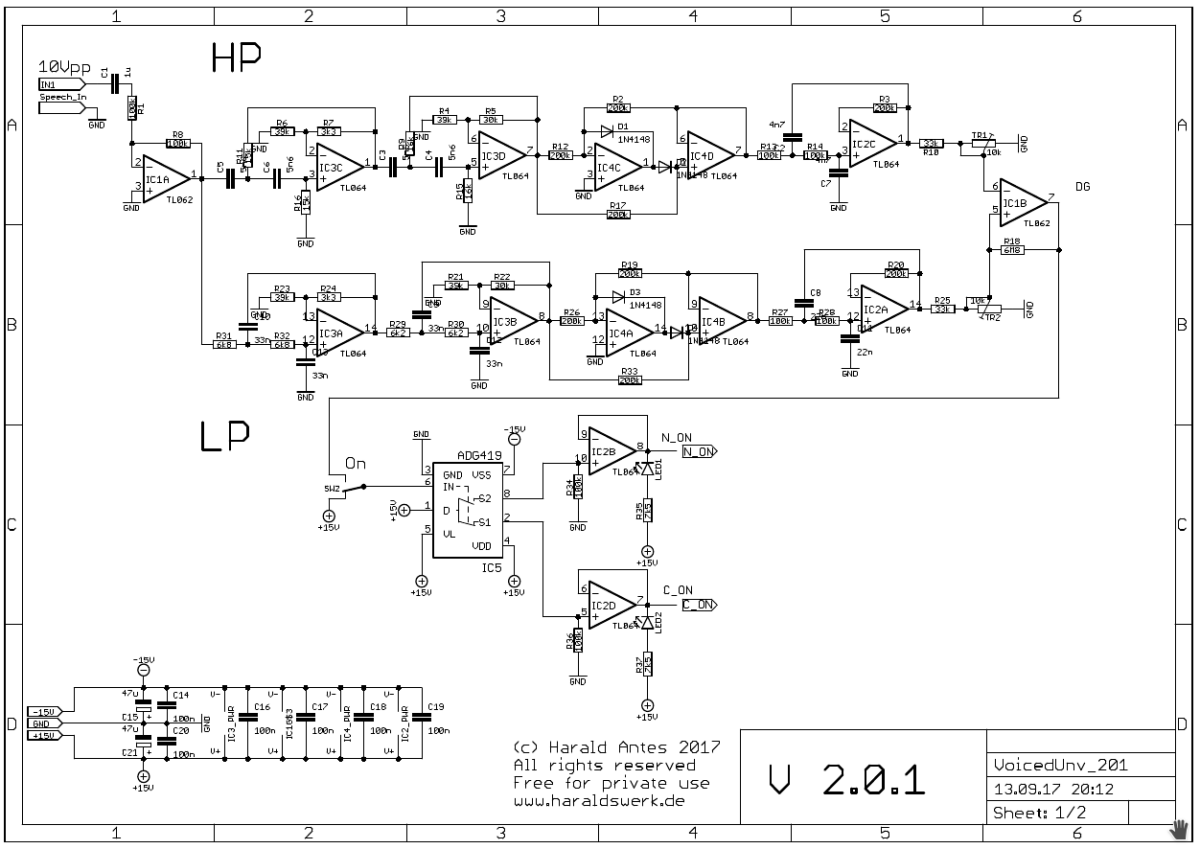
36dB VCF LP/HP schematic page one
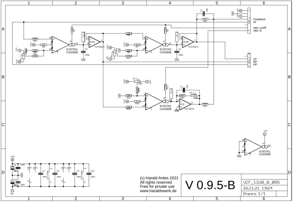
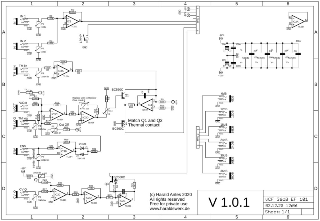
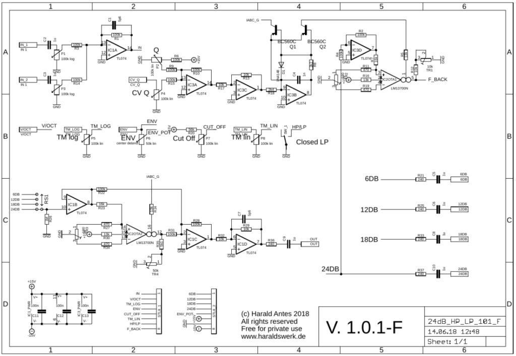
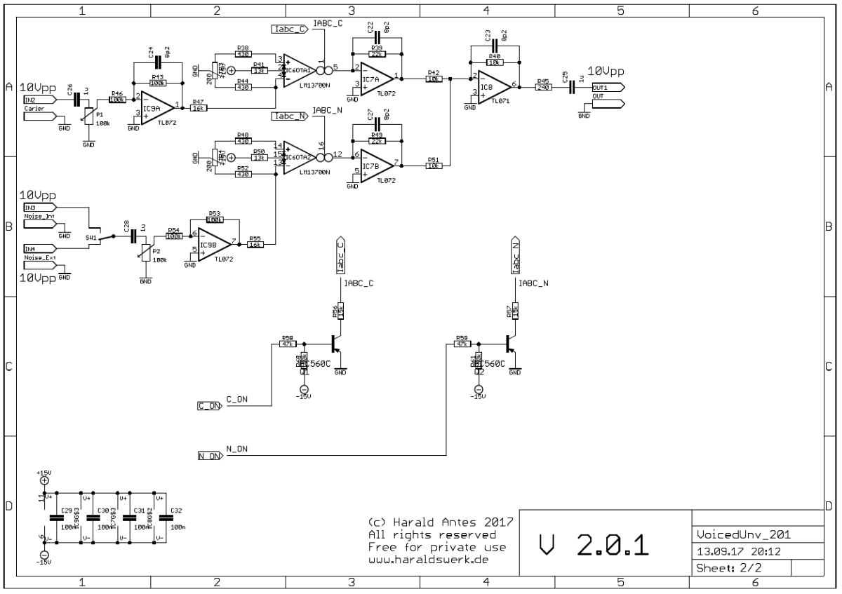
Straight forward design. Six state variable filter cells are connected together in series, The output of each filter cell is brought out. There are a lot descriptions of those state variable filters out there. I feel no need to add another one. The resonance (Q) is voltage controlled with means of the OTA IC16OTA2 in the upper right corner (page 1). To compensate the volume loss when the resonance (Q) is turned up a second OTA (IC16OTA1) is used. This two OTA shares the same Iabc source. The amplification of this second OTA is increased when Q is going high and add volume to the output signal (See page 2 of the schematic).
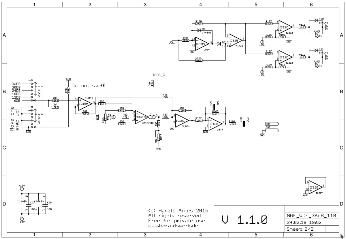
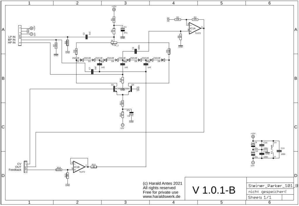
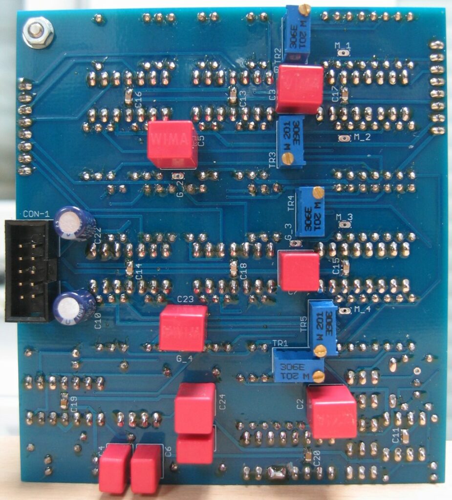
36dB VCF LP/HP schematic page two
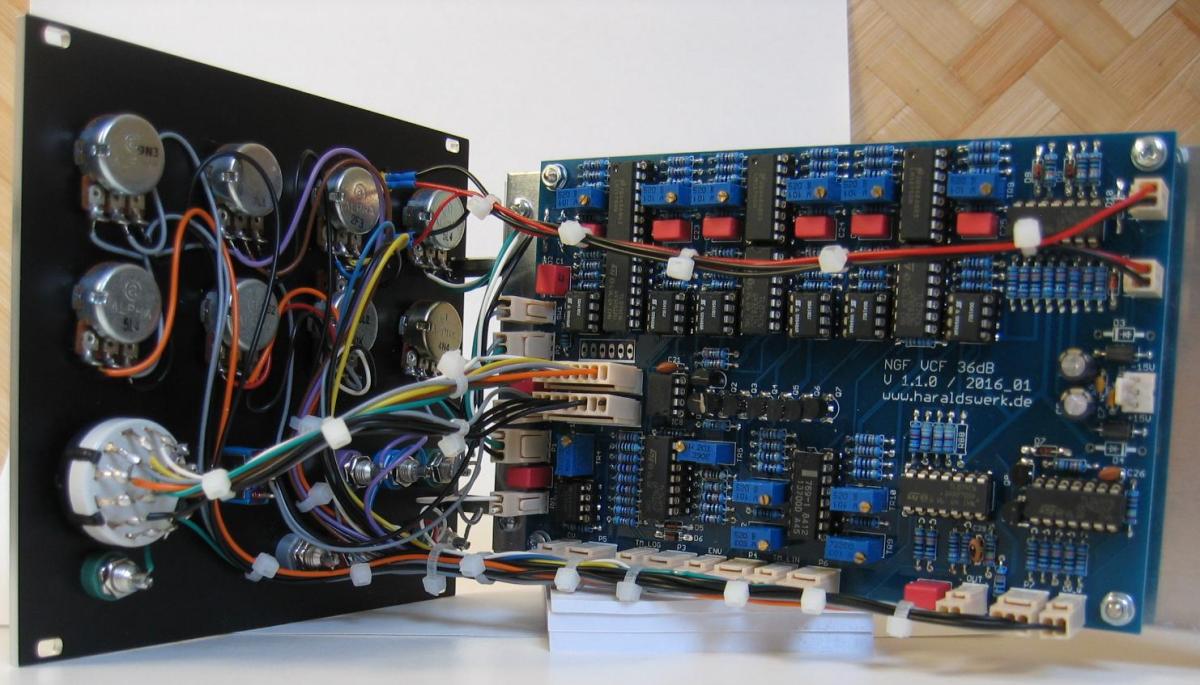
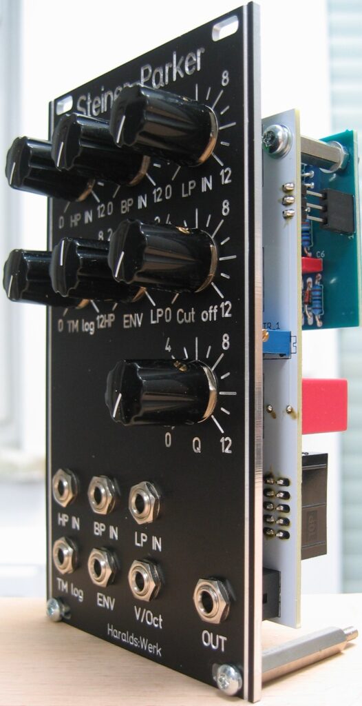
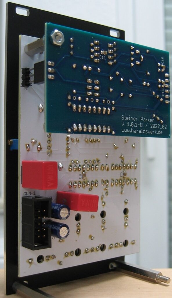
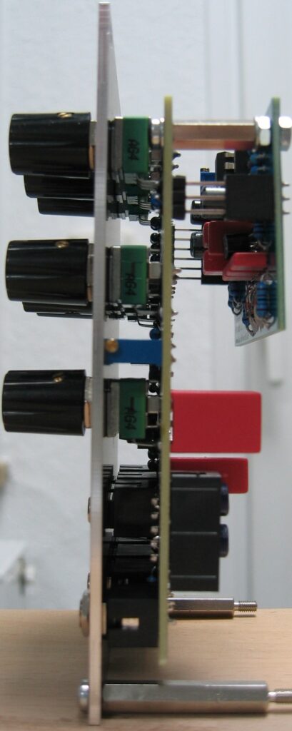
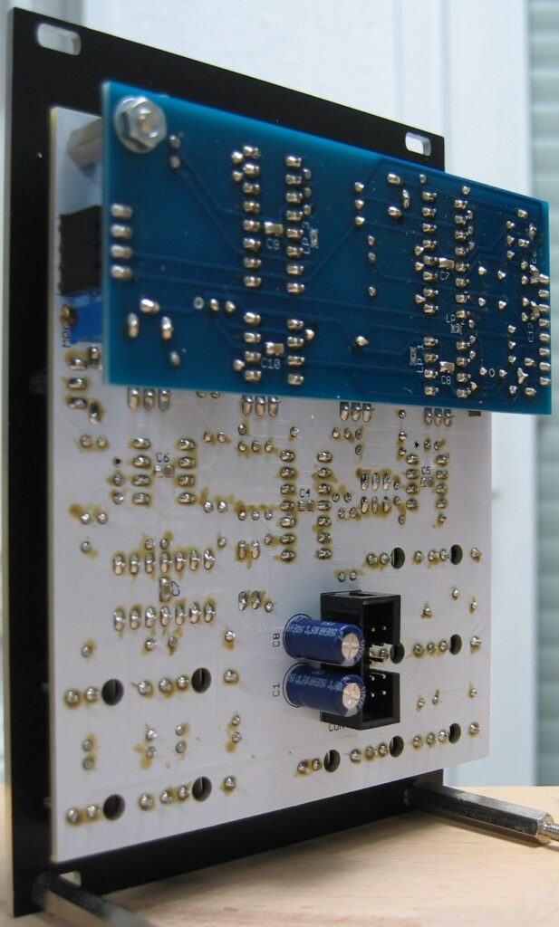
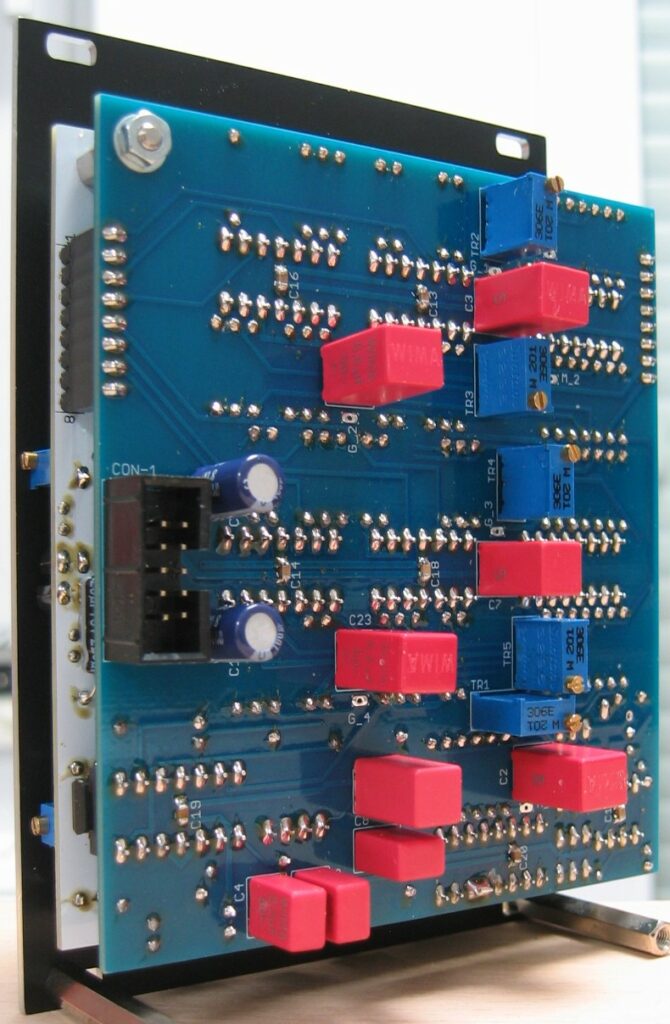
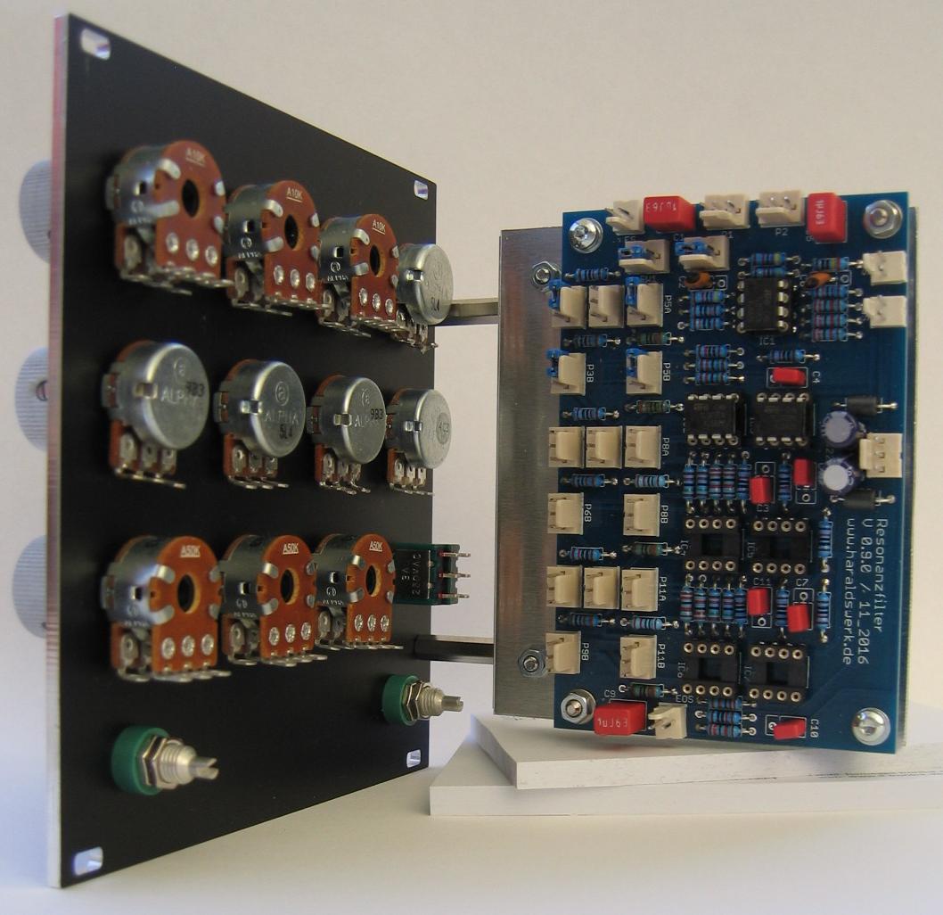
36dB VCF LP/HP module back view
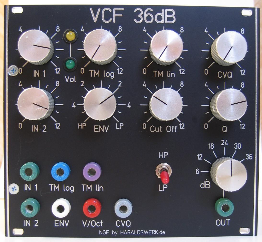
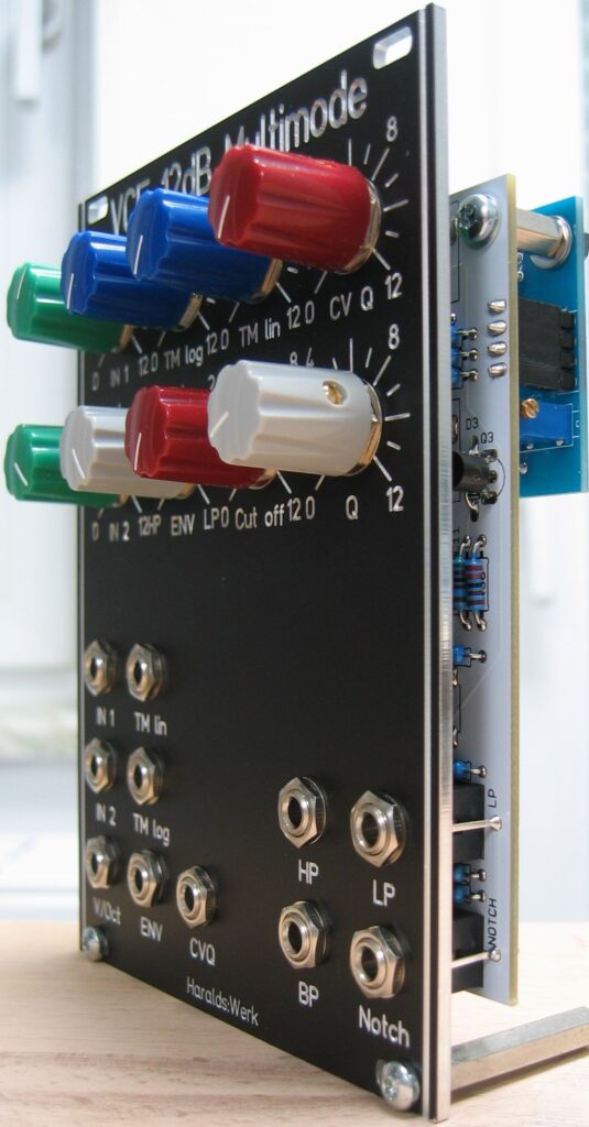
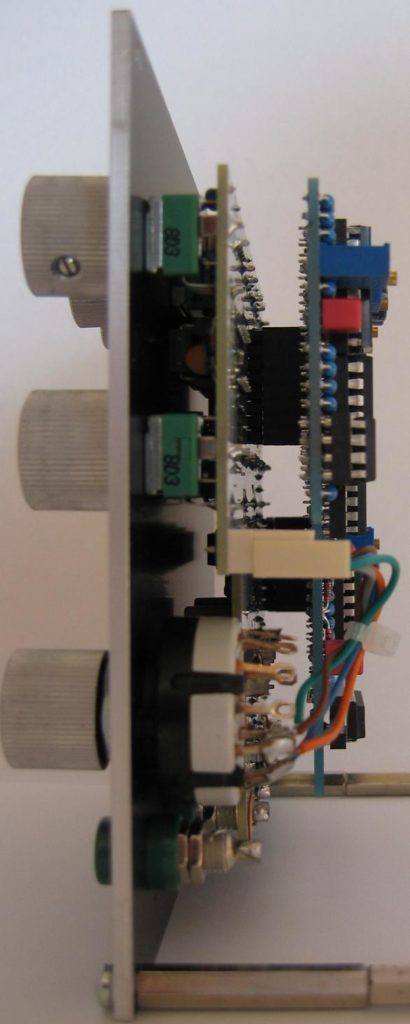
36dB VCF LP/HP module front