Quad Ringmodulator

Quad Ringmodulator: Front view

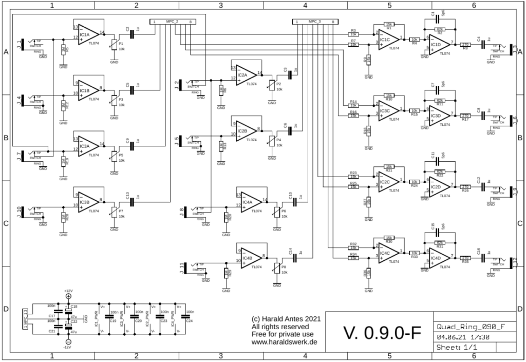
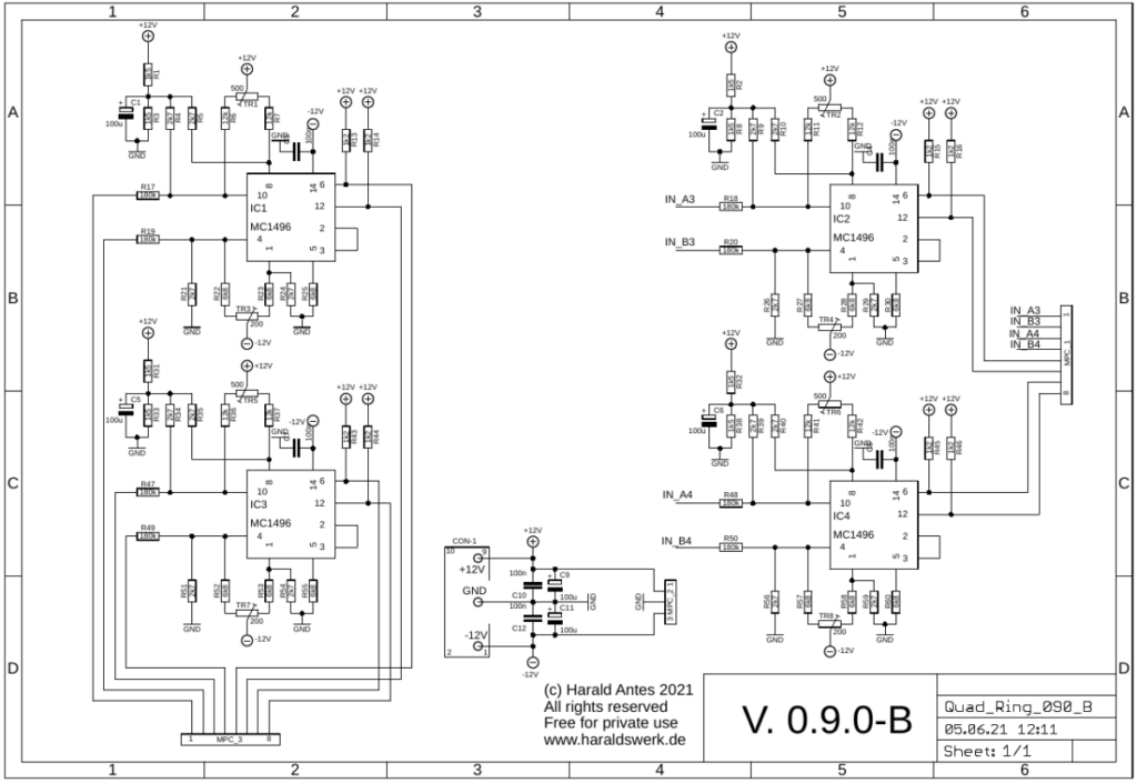
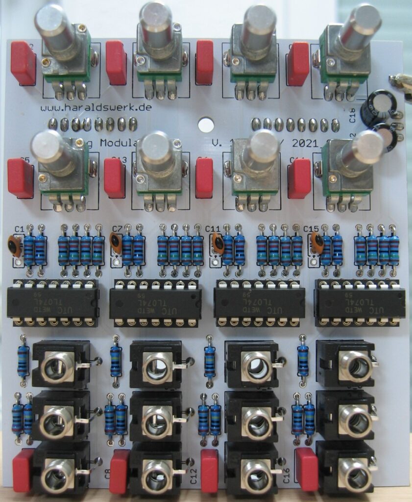
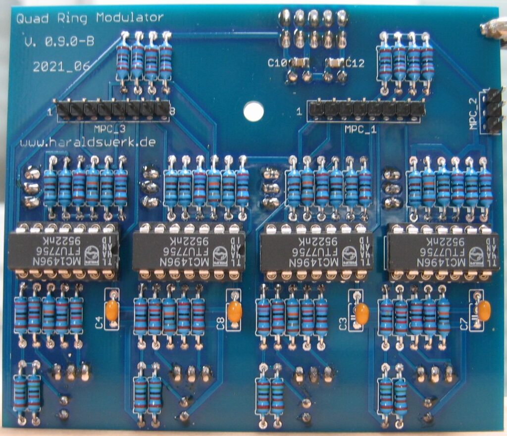
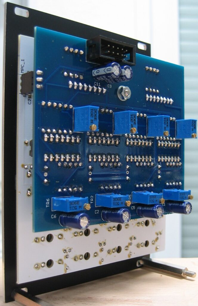
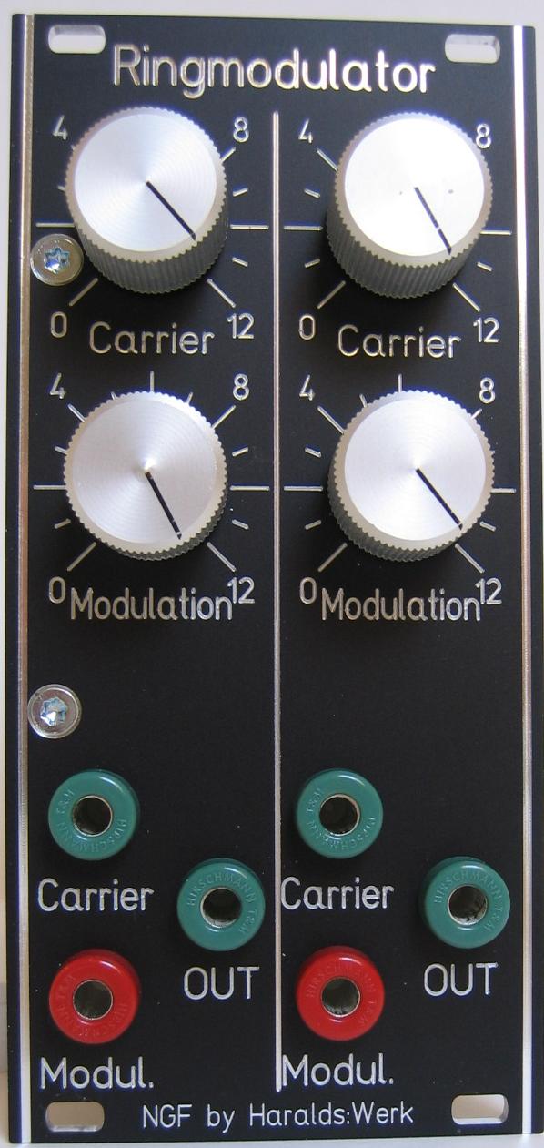
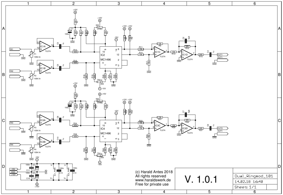
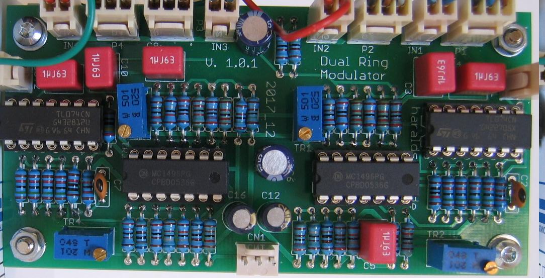
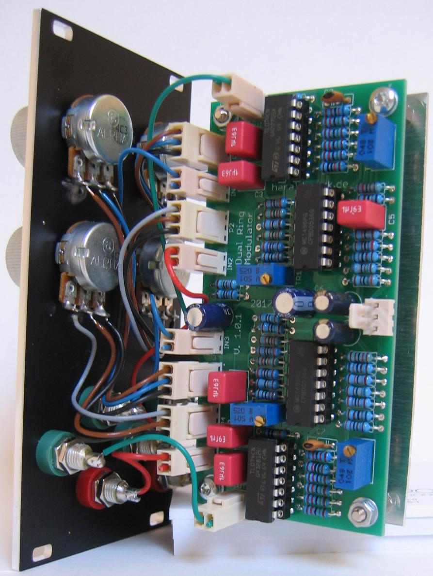
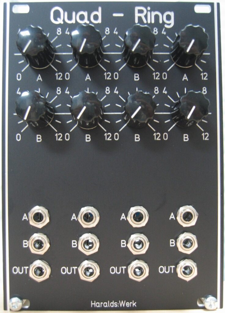
This is the 12V Euro version of my NGF dual version. It uses the now obsolete LM1496 balanced modulator -demodulator. But you can still source them and I have some in my stock. So I decided to make a PCB and module. I started with the original Elektor Formant schematic published in “Formant Erweiterungen” p35ff. I left out the microphone and envelope follower part because I already have such modules. I have added input buffers and raised the signal level to my 10Vpp used throughout my system.

Specs and features

  • Quad Ringmodulator
  • 10Vpp input and output
  • Runs on +/-12V and +/-15V
  • Power consumption around 70mA each rail

The documentation and the Gerber files for download can be found in my website.

Quad Ringmodulator: Schematic control board
Quad Ringmodulator: Schematic main board
Quad Ringmodulator: Populated control PCB
Quad Ringmodulator: Populated main PCB
Quad Ringmodulator: Back view
Quad Ringmodulator: Side view

Track (Sample) and Hold

Track (Sample) and Hold: Front view

One more module for my Shakuhachi to Synths project. Not exclusively of course. This is a Track and Hold. Which is quite useful for other patches as well. In the Shakuhachi patch it is used to suppress an incomplete pitch to voltage conversion from the Pitch to voltage converter when the player stops blowing. The module tracks the incoming (control) voltage as long as the gate input is high. When the gate goes low the output voltage is kept. The module is DC coupled to track slowly moving voltages. For this one I have used some obsolete parts, which I had laying around. So, if you want to build it, make sure that you can get those parts. You can use it as Sample and Hold as well. Instead of a gate apply a trigger at the gate input.

Specs and features

  • Track or Sample and Hold
  • DC coupled
  • Gate input with LED
  • Signal input
  • Signal output
  • Threshold
  • Runs on +/-12V and +/-15V
  • Power consumption below 20mA each rail

The documentation and the Gerber files for download can be found in my website.

Track (Sample) and Hold: Schematic
Track (Sample) and Hold: Populated PCB
Track (Sample) and Hold: Back view
Track (Sample) and Hold: Side view

ADSR Euro-rack

ADSR: Front view
ADSR: Front view

This is another derivation off the ADSR for my NGF-E project, adapted to 12V Euro-rack format. Because this one is a stand alone module I have removed all additional features from the Next Generation Formant project. Nonetheless it is still based on original Elektor Formant ADSR schematic. I made some error corrections and added my changes to the design. All parts are updated to today (2021/01) available parts. I have made a few changes to fix some shortcomings of the original. A triple range switch was added for finer adjustment of the ADSR CV-output signal. The attack rise time is shorter now as in the original. The gate input is buffered. The fixes a fault in the original when working with analog sequencers. The output voltage is slightly raised to reach really 5V. Due to the design of the original Elektor Formant ADSR the output of the original ADSR keeps a residual voltage of about 0,5V. I have put an compensation in my design to correct this. The driver circuitry for the output indicator LED is changed for better linearity.

Specs and features

  • AD/ADSR switch
  • Gate input 5V
  • CV output ..5V
  • CV output indicator
  • Range switch: fast, middle, long
  • Attack (A) 0,5ms…16s
  • Decay (D) 4ms…40s
  • Sustain (S) 0..5V
  • Release (R) 4ms..40s
  • Power consumption below 15mA each rail

The documentation and the Gerber files for download can be found in my website.

ADSR: Schenmatic main PCB
ADSR: Schematic main PCB
ADSR: Schematic control PCB

This is a close clone of the Elektor Formant ADSR. Here i only describe the changes i have made. The description of the other parts of the circuitry can be found in the original Elektor Formant documentation. The gate signal input resistance is raised from 33kOhm to 1megOhm with the input buffer IC1A. This protects against double triggering with the falling edge of the gate signal when using sequencers. R30 is used to fix the input to a defined potential when no signal is attached to the input. C1 was lowered to 6n8 from 10nF. In combination with C2 and the raised charging voltage through IC1B/R9 this makes for faster attack time. The load capacitor of 10u was replaced with three selectable capacitors of 2,2uF 4,7uF and 10uF. This makes for a finer adjustment of the response times of the ADSR. The voltage divider R19/R21 was adjusted to ensure that the output level of 5V is reached. If this feature is not used R25 should be lowered to 5k1. Construction conditioned the output at IC1D only reaches a minimal voltage of about 0,5V. To compensate for this i added IC2A. If the ADSR is not used the output voltage is now at -0,5V. The current consumption was lowered with using the TL064 and a low current LED.

ADSR: back view
ADSR: Back view
ADSR: Populated main PCB
ADSR: Populated control PCB
ADSR: Side view
ADSR: Side view

VCA Sims / flat Version

VCA Sims - flat Version

VCA Sims – flat Version

This is the flat Version of my Sims VCA. The original Elektor Formant VCA used two 3080 in series. In most cases only one is used and the second one only adds to noise and distortion. This VCA is AC coupled only. The THD in the Elektor Formant VCA is about 1% and the noise to voltage ratio is not that good either. Time to look for a replacement. I wanted a decent DC coupled audio VCA to process audio as well as control voltages. And easy available parts (2014/08). I tried different architectures and then decided to separate audio and DC VCA. With specialized VCA it is easier to reach both goals. I made my own implementation of the Sims-VCA introduced by Mike Sims in the EDN Magazine January 1995. With this architecture it is possible to achieve THD of 0,02%. Unfortunately i can not confirm the statement from Mike Sims that trimming the circuit for minimum THD achieves minimum control voltage feedthrough. Trimming for minimum THD causes an constant DC bias at the output. I have had to add a output capacitor to avoid the bias at the output. And you need test equipment to measure the THD for correct trimming. If you can not measure THD better build my DC_VCA. You can achieve 0,2 % THD here. Still good.

Specs and features:
• AC coupled 0,02% THD
• lin and log response
• CV 0..+5V
• 5Vpp in- and output

The documentation for download can be found in my website.

VCA Sims schematic back PCB

VCA Sims schematic back PCB

VCA Sims schematic front PCB

VCA Sims schematic front PCB

Please refer to my first implementation (link) or the original article from Mike Sims

VCA Sims side view

VCA Sims side view

VCA Sims side view

VCA Sims side view

Output Module

Output Module: Front view

Output Module: Front view

This is my replacement of the original Elektor Formant COM module. I discarded the original circuitry because of the TL085 used with his unusual pinout and the availability of dedicated audio operational amplifiers. I used a more effective filter implementation for tone control. The tone control is derived from “Small Signal Audio Design” by Douglas Self Chapter 15. A optional level indicator makes it easier to find the right volume level for best SNR. The maximum output volume is adjustable to protect your PA. You can connect the output directly to active monitors.

Specs and features
• Bass, middle, treble tone control
• Adjustable maximum output volume
• Optional volume indicator
• Direct connection to active monitors
• Runs on +/-15V and +/-12V (with minor resistor changes)

The documentation for download can be found in my website.

Output Module: Schematic front PCB

Output Module: Schematic front PCB

Output Module: Schematic back PCB

Output Module: Schematic back PCB

A description can be found in “Small Signal Audio Design” by Douglas Self Chapter 15

Output Module: Stuffed PCB back view

Output Module: Stuffed PCB back view

Output Module: Stuffed PCB side view

Output Module: Stuffed PCB side view

Output Module: Side view

Output Module: Side view

NGF Project: Dual Sample and Hold

Dual Sample and Hold: front view

Dual Sample and Hold: front view

Storing analog signals is a often used function in analog synthesizers. This sample and hold implementation follows closely the original Elektor Formant version of Book 2 “Formant Erweiterungen” p84ff. It is build for my Next Generation Formant project. Because I use the LM13700 here as replacement for the CA3080 I have build a dual sample and hold version. The PCB size is reduced from 100x160mm for a single version to 50x70mm for the dual version.

Specs and features
• Dual sample and hold
• 10Vpp input and output
• Runs on +/-15V and +/-12V
• Power consumption below 25mA each rail

The documentation for download can be found in my website.

Dual Sample and Hold: schematic

Dual Sample and Hold: schematic

This implementation follows closely the original Elektor Formant implementation. Refer to the original documentation if needed. You can find it on the net. My changes are the input buffers, using the LM13700 instead of the CA3080 and the adaption to my 10Vpp signal level.

Dual Sample and Hold: populated PCB

Dual Sample and Hold: populated PCB

Dual Sample and Hold: back view

Dual Sample and Hold: back view

NGF Project: 440CPS

NGF-E Project: 440CPS front view

NGF-E Project: 440CPS front view

Not much to say. A 440CPS module. Quite useful for tuning in a bigger system. OK, one more sentence. It is the replacement for the 440CPS module from the Elektor Formant in my Next Generation Formant project Project.

Specs and features
• On/Off Switch to keep the 440Hz out of the system when not needed
• Runs on +/-15V and +/-12V
• Power consumption below 25mA +rail / 5mA -rail

The documentation for download can be found in my website.

NGF-E Project: 440CPS schematic

NGF-E Project: 440CPS schematic

Everything is done in software. Output is a 440Hz Square wave. That’s it.

NGF-E Project: 440CPS populated PCB

NGF-E Project: 440CPS populated PCB

NGF-E Project: 440CPS back view

NGF-E Project: 440CPS back view

NGF-Project: Elektor Wave Processor

NGF Project: Elektor Wave Processor

NGF Project: Elektor Wave Processor

A small but very versatile module. It is derived from the original Elektor Formant book “Formant Erweiterungen” p87 ff. Some resistor values are changed to handle the 10Vpp signal level of my system. You can shape the input signal in many ways. You can clip the signal. You can fold the signal. You can emphasize the third harmonic. You can unsymmetrical emphasize the clipped and unclipped signal. You can reverse the input signal. The clipping level is voltage controlled.

Specs and features

• Clipping the signal
• Folding the signal
• Emphasize the third harmonic
• Unsymmetrical emphasize the clipped and unclipped signal
• Clipping level voltage controlled
• 10Vpp input and output
• Runs on +/-15V and +/-12V

The documentation for download can be found in my website.

NGF Project: Elektor Wave Processor, schematic

NGF Project: Elektor Wave Processor, schematic

This implementation follows closely the original Elektor Formant implementation. Refer to the original documentation if needed. You can find it on the net. My changes are the adaption to my 10Vpp system signal level.

NGF Project: Elektor Wave Processor, populated PCB

NGF Project: Elektor Wave Processor, populated PCB

NGF Project: Elektor Wave Processor, rear view

NGF Project: Elektor Wave Processor, rear view

NGF Project: Dual Ringmodulator

NGF Project: Dual Ringmodulator front view

NGF Project: Dual Ringmodulator front view

I was a bit hesitant doing this module because it uses the now obsolete LM1496 balanced modulator-demodulator. But you can still source them and I have some in my stock. So I decided to make a PCB and module for my Next Generation Formant project. I started with the original Elektor Formant schematic published in “Formant Erweiterungen” p35ff. I left out the microphone and envelope follower part because I already have such modules. I have added input buffers and raised the signal level to my 10Vpp used throughout my system. I was able to put two ringmodulator on a 50x100mm PCB.

Specs and features
• Dual ringmodulator
• 10Vpp input and output
• Runs on +/-15V and +/-12V

The documentation for download can be found in my website.

NGF Project: Dual Ringmodulator schematic

NGF Project: Dual Ringmodulator schematic

This implementation follows closely the original Elektor Formant implementation. Refer to the original documentation if needed. You can find it on the net. My changes are the input buffers and the adaption to my 10Vpp signal level.

NGF Project: Dual Ringmodulator populated PCB

NGF Project: Dual Ringmodulator populated PCB

NGF Project: Dual Ringmodulator back view

NGF Project: Dual Ringmodulator back view

NGF LFO: flat Version

NGF LFO flat version side view

NGF LFO flat version side view

This is the LFO module for my Next Generation Formant project. It provides triangle, ramp up, ramp down and square wave output (-5V to +5V). This design follows closely the original from the Elektor Formant.
Most noticeable change is moving to a “flat” design. The depth of the module is significantly reduced and most important no more potentiometer wiring is needed!

The documentation for download can be found in my website.

LFO flat Version Schematic back PCB

LFO falt Version Schematic back PCB

LFO flat Version Schematic front PCB

LFO flat Version Schematic front PCB

The oscillator consists of an integrator IC1A and an OpAmp Schmitt-Trigger IC1B. The triangle wave of the oscillator arises through the feedback of the trigger output to the input of the integrator. At the integrator output IC1A arises a triangle with the amplitude of the hysteresis of the Schmitt-Trigger. The input voltage of the integrator sets the rise and fall time of the voltage output. The square wave output is buffered with IC1C. The circuitry around IC1D provides the saw output. IC3C inverts the saw.

LFO flat Version populated front PCB

LFO flat Version populated front PCB

LFO flat Version populated back PCB

LFO flat Version populated back PCB

LFO flat Version faceplate

LFO flat Version faceplate