Dual Bernoulli Gate (Either/Or)

Bernoulli Gate: Front view

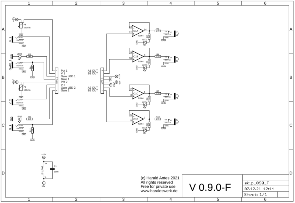
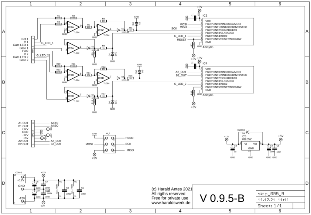
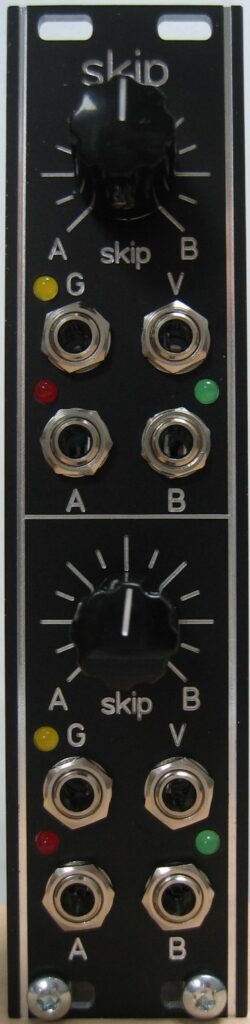
This module takes the incoming gate or trigger and routes it to either of its two outputs. The distribution is software driven, according to a random coin toss. You can select the probability distribution with a potentiometer and an input control voltage. The potentiometer voltage and the control voltage are added together. The probability goes from 0% to 100% at output A and from 100% to 0% on output B.

Specs and features

  • Randomly skip Gates and Triggers
  • Probability distribution voltage controlled
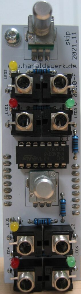
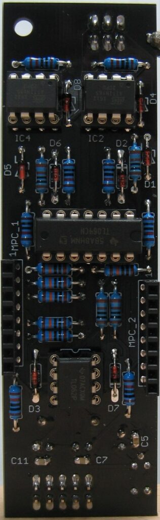
  • Dual Bernoulli gate
  • Runs on +/-12V and +/-15V
  • Power consumption below 20mA positive rail. 5mA negative rail.

The documentation and the Gerber files for download can be found in my website.

Bernoulli Gate: Schematic control board
Bernoulli Gate: Schematic main board
Bernoulli Gate: Populated control board
Bernoulli Gate: Populated main board
Bernoulli Gate: Halve back view
Bernoulli Gate: Side view

Quad white and colored noise source. Quad random voltage source

Quad white and colored noise source. Quad random voltage source. Schematic control PCB
Quad white and colored noise source. Quad random voltage source: Front view

It is quite useful to have different adjustable noise and random voltage sources. Depending on your patch stile of course. Here is the quad version of my noise module from the NGF project. It is a combination of two original Elektor Formant modules. The noise module from Elektor Formant book one and the colored noise (CNC) module from book two. It provides four independent white noise outputs, four adjustable colored noise outputs with “red” and “blue” adjustment. The four random voltage outputs are adjustable in speed of change. The noise is derived from the reverse biased BE diode of an NPN transistor.

Specs and features

  • Four independent white noise outputs
  • Four independent adjustable colored noise outputs with “red” and “blue” adjustment
  • Four random voltage outputs, adjustable in speed of change
  • Four LED indicating the random voltage change
  • Runs on +/-12V and +/-15V
  • Power consumption around 65mA each rail

The documentation and the Gerber files for download can be found in my website.

Quad white and colored noise source. Quad random voltage source. Schematic control PCB
Quad white and colored noise source. Quad random voltage source: Schematic control PCB
Quad white and colored noise source. Quad random voltage source. Schematic main PCB

Description:

(Given for one of the four.) Noise source is the reverse biased BE diode of NPN transistor Q1 (B_090). The following operational amplifier IC1A and IC1B (B_090) amplifies the noise to 10Vpp. IC1C (B_090) is the buffer for the white noise output. IC2B (F_101) is configured as a 12dB low pass. So you get a low frequency random voltage. The changing speed is set with P3A/P3B (F_101) which sets the corner frequency of the low pass filter. IC2A / LED1 (F_101) makes the fluctuation visible. TR_1 (F_101) adjust the brightness of LED1 (F_101). In the feedback loop of IC1B (F_101) is an adjustable filter combination which gives you a wide range of adjustable colored noise with P1 and P2 (F_101). The output is buffered with IC1A (F_101).

Quad white and colored noise source. Quad random voltage source. Populated control PCB
Quad white and colored noise source. Quad random voltage source. Populated main PCB