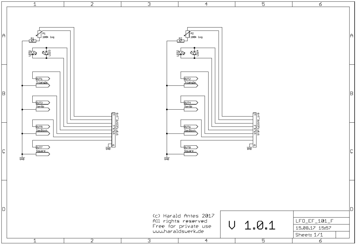
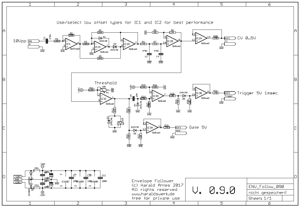
This envelope follower was first build for my Shakuhachi 2 Synth project. But it is useful for any other input signal which you want to derive a control voltage from. It provides a gate and a trigger signal as well. The envelope follower is used to detect the amplitude variations of the incoming signal and produces a control voltage that resembles the variations in the input signal.
The gate and trigger signal is derived from the input signal as well. You can vary the threshold to determine at what minimum signal level the gate goes high and the trigger fires. Gate level is +5V. Trigger level is +5V/1msec.
NGF Project: Envelope follower
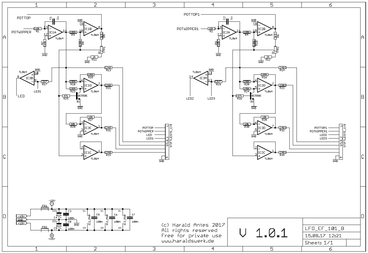
The incoming signal is rectified with a precision full wave rectifier. Then feed to a low pass filter for smoothing. The given filter values here are optimized for use with the Shakuhachi, but can easily changed to your needs. The filter values affect the ripple and the timing of the output control voltage.
The gate and the trigger signal is derived from the filter output with means of a comparator. You can adjust the sense level with the threshold potentiometer. The gate is indicated with a LED. The trigger pulse is derived from the gate with an differentiator.
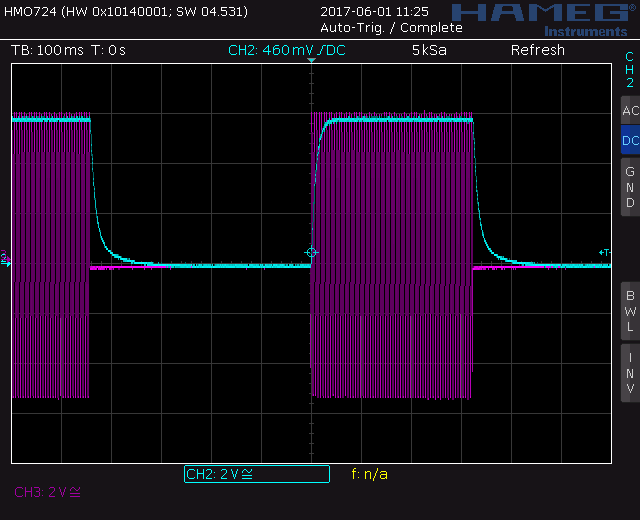
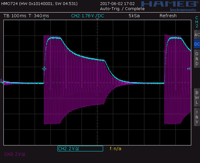
Envelope follower: Scope picture with square cv
The picture above shows the control voltage of the envelope follower following a signal of 200Hz sine wave from a VCA (purple line) with a square control voltage (blue line).
Envelope follower: Scope picture with ADSR cv
The picture above shows the control voltage of the envelope follower following a signal of 200Hz sine wave from a VCA with a control voltage set by an ADSR.
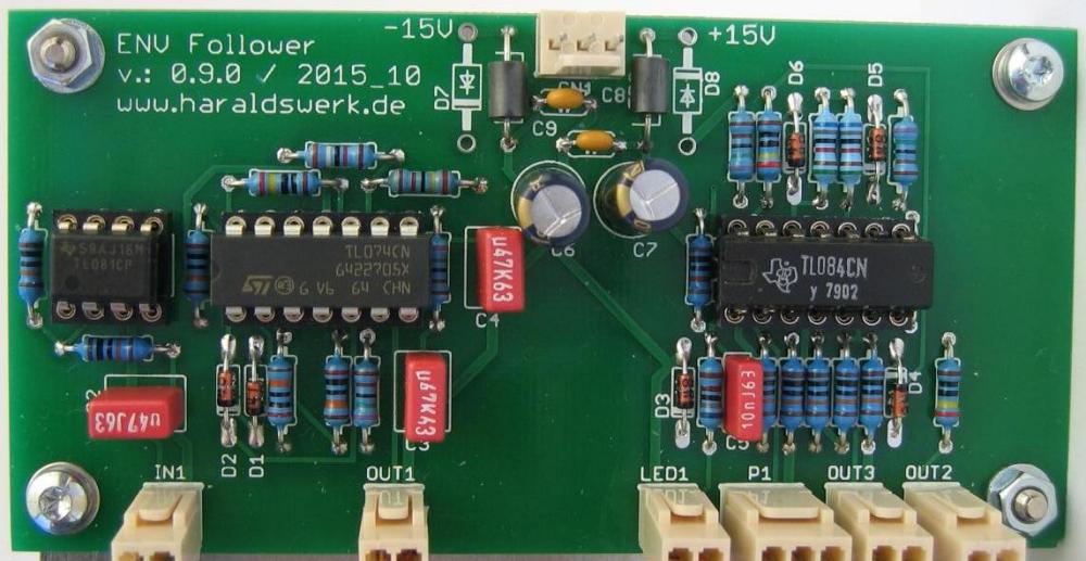
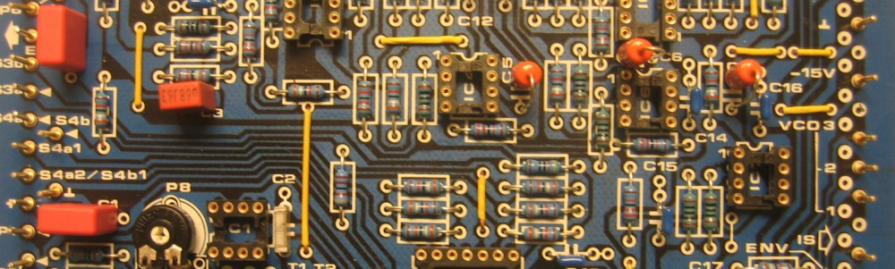
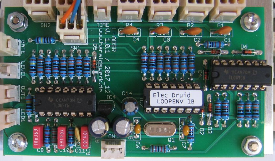
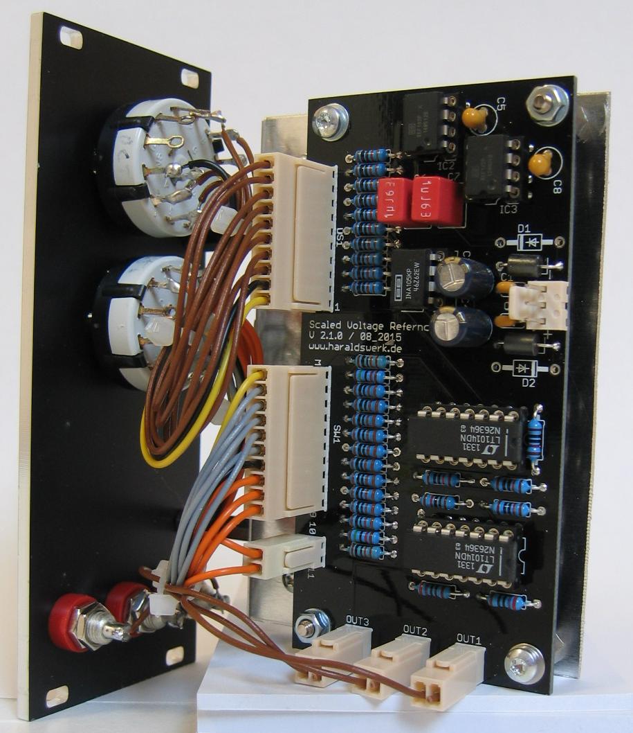
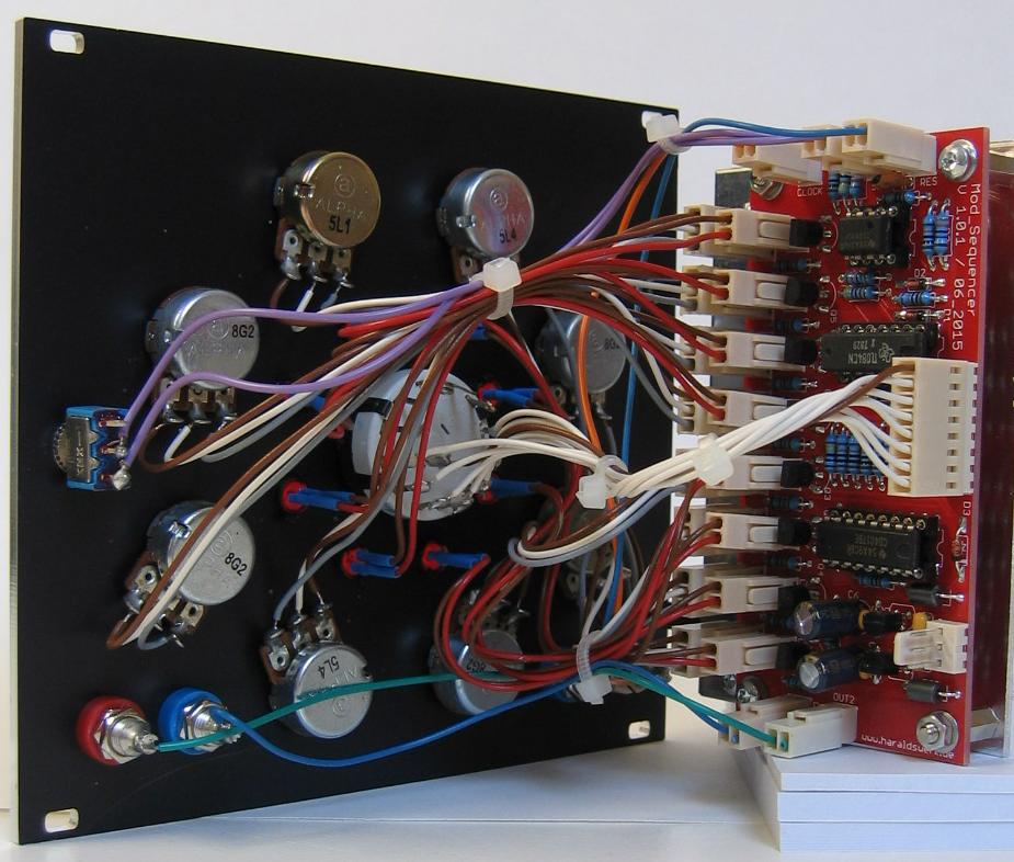
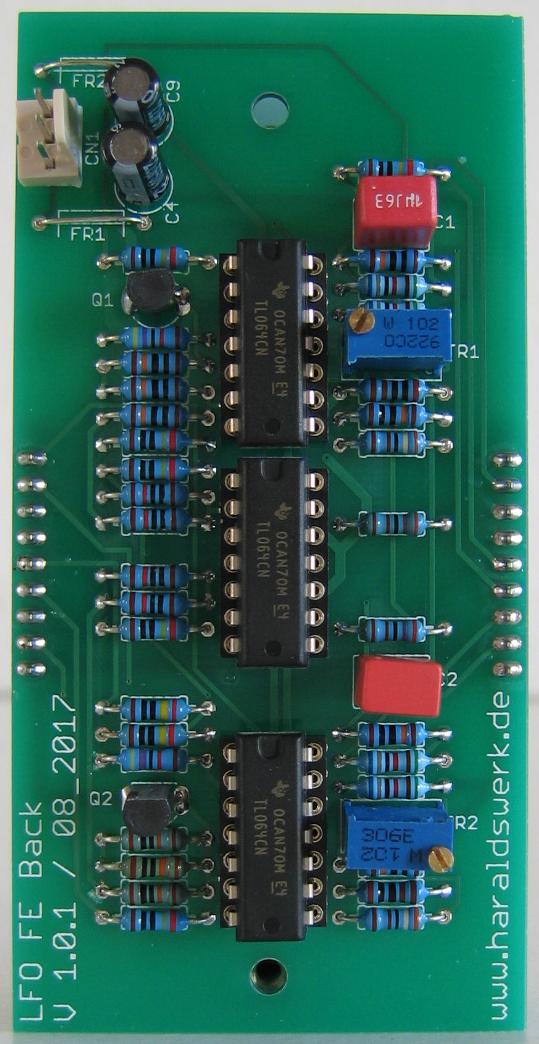
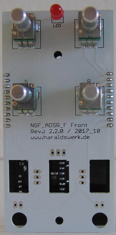
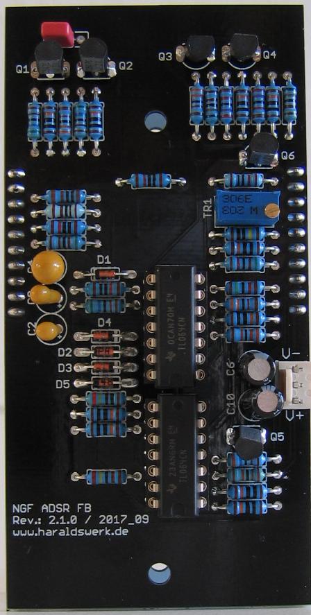
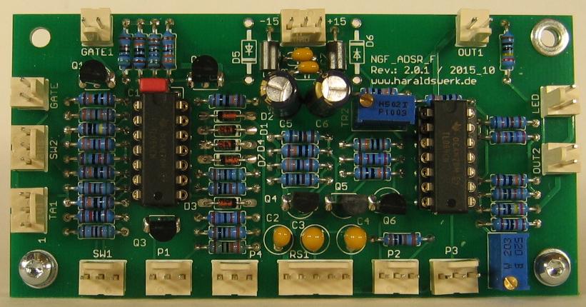
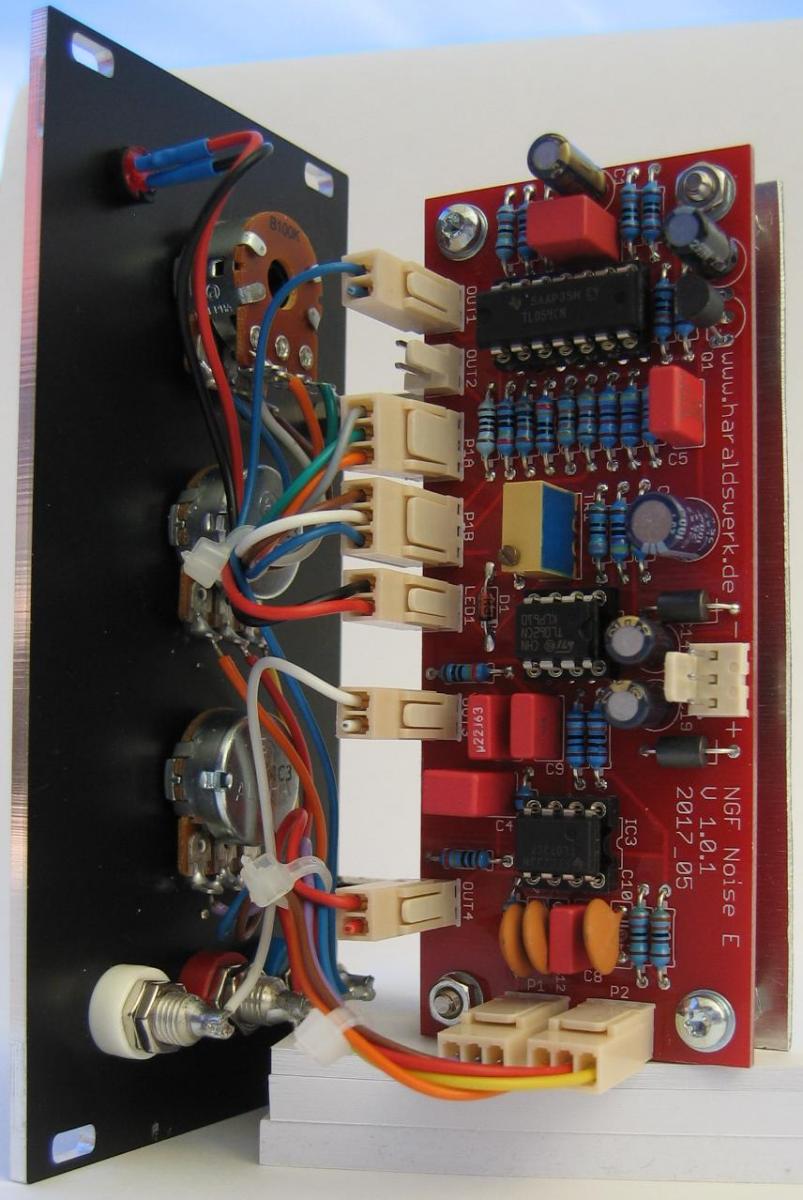
Envelope follower: stuffed PCB
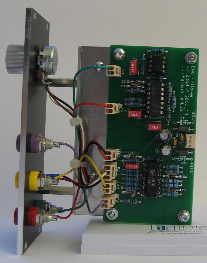
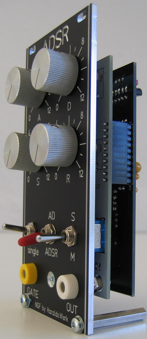
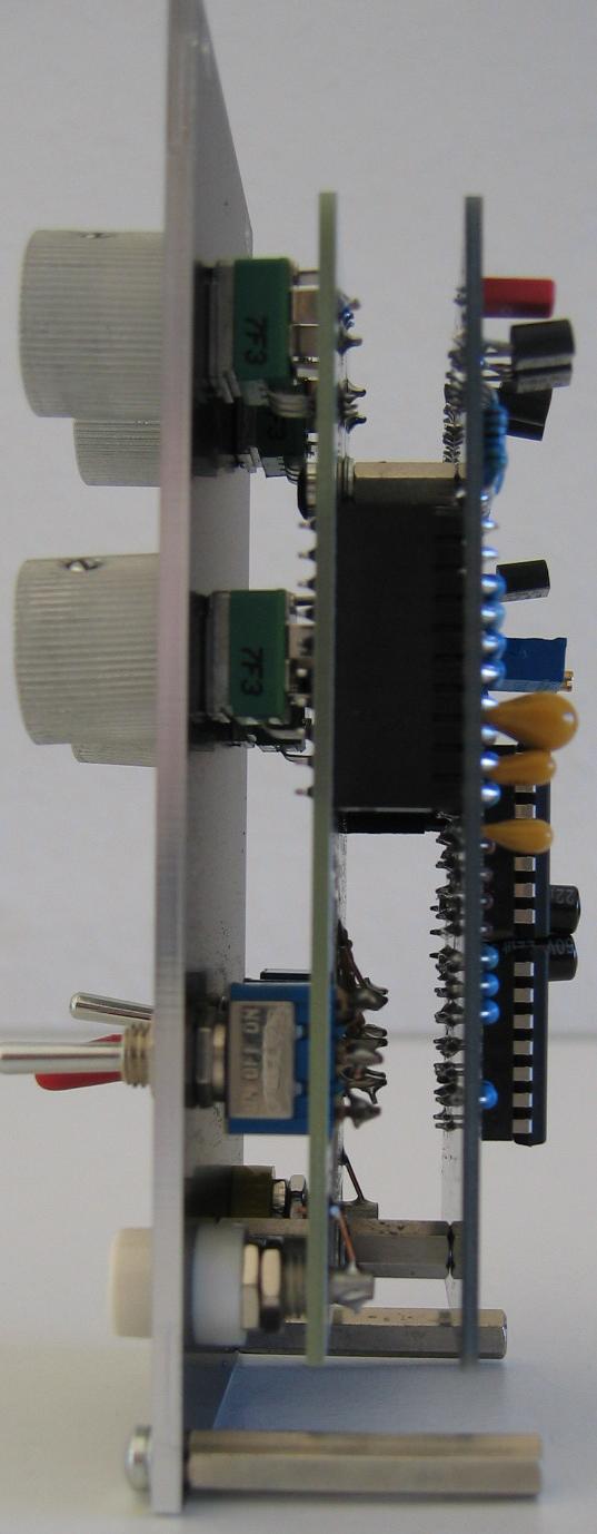
Envelope follower: Module
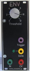
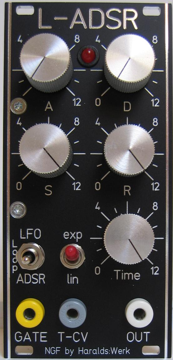
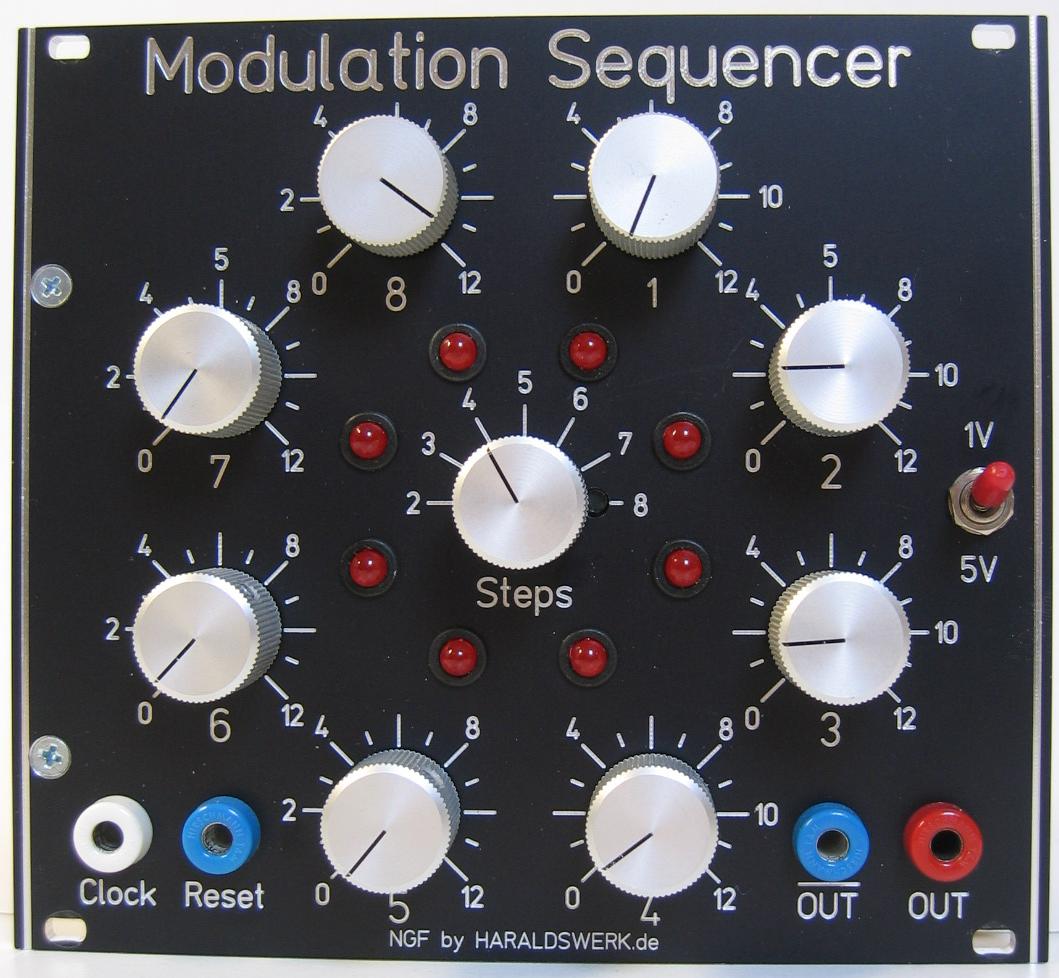
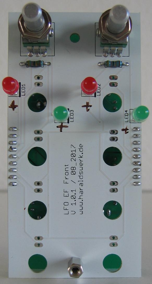
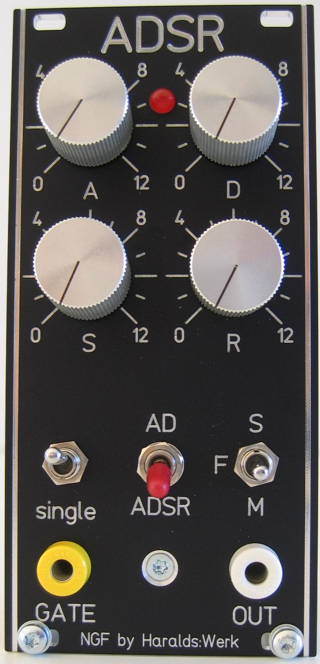
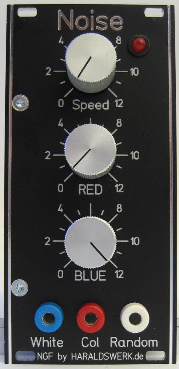
Envelope follower: Front