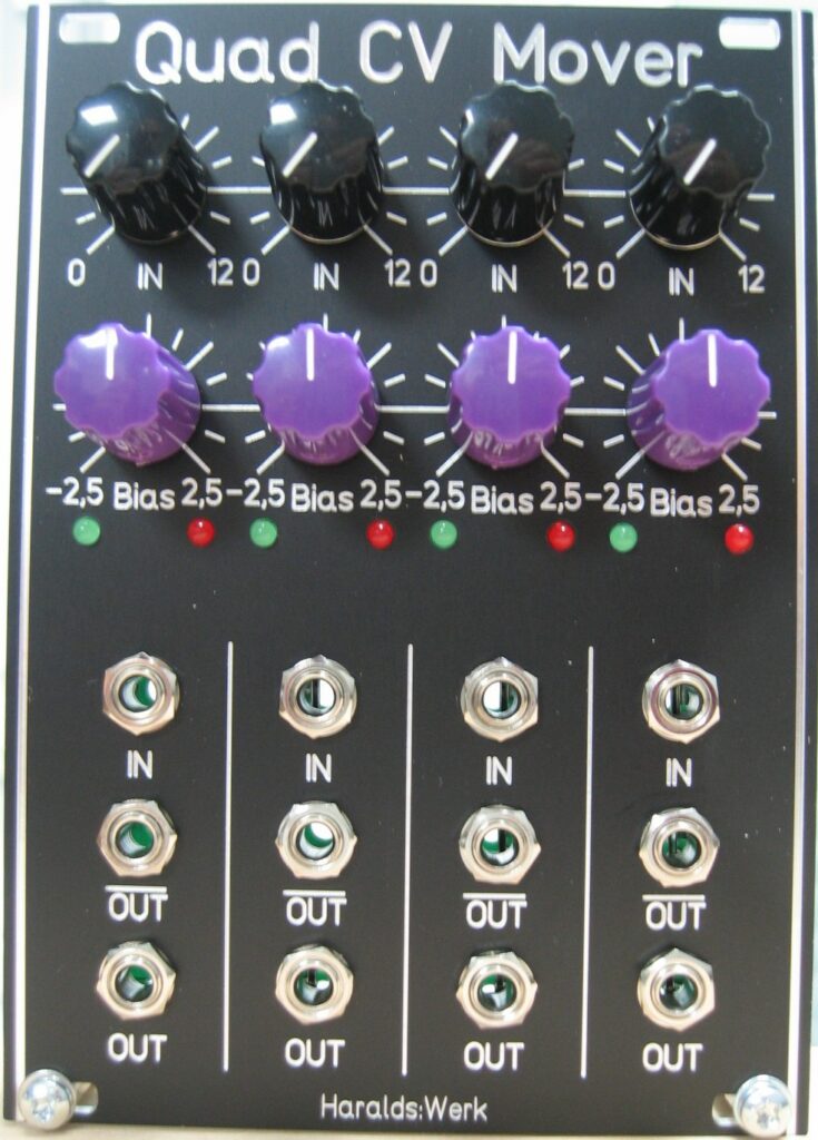
A companion for my other quad modules. Especially for my Quad LFO. You can use it as attenuator, attenuverter, CV Source and, most important, for offsetting bipolar control voltages to make them unipolar, positive or negative. The module is DC coupled, so you can use it for DC and AC. It is possible to offset the input with +/- 2.5V. The offset is signaled with diodes. There is an inverted output added as well. The main usage is for processing bipolar LFO voltages into unipolar control voltage inputs. If you have a LFO with +/- 5V output and want to make it unipolar set the input to halve and the offset to +2.5V. The output is then from 0..5V and 0..-5V at the negative output. You can easily adapt the module to other offset voltages with a few resistor changes.
Specs and features
Attenuator
Inverted and non- inverted output
Attenuverter
+/- 2.5V offset
Runs on +/-12V and +/-15V
Power consumption below 20mA each rail
The documentation and the Gerber files for download can be found in my website.
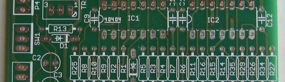
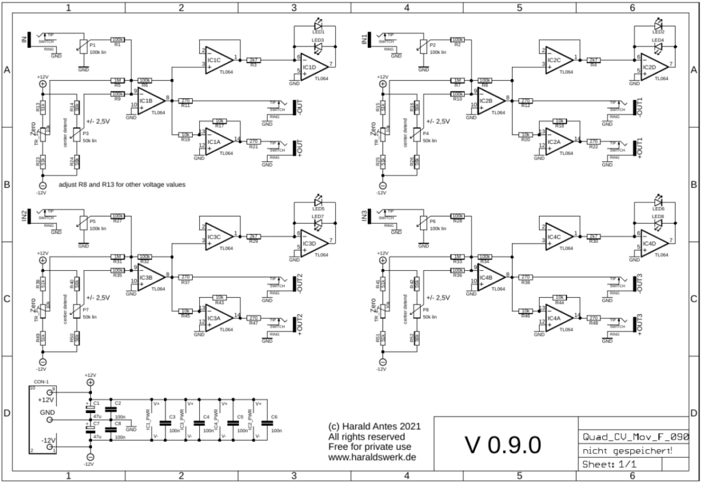
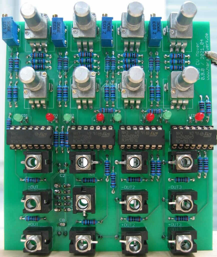
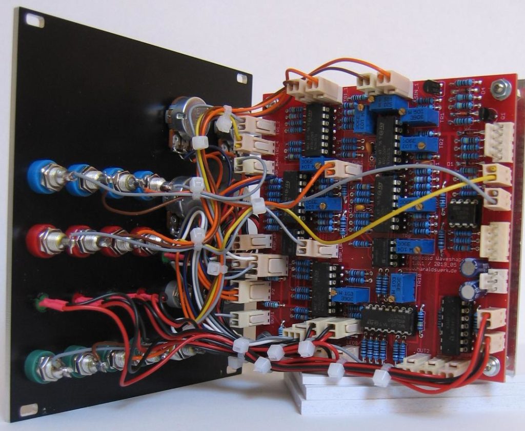
CV Mover quad: SchematicCV Mover quad: Populated PCBCV Mover quad: Back viewCV Mover quad: Side view
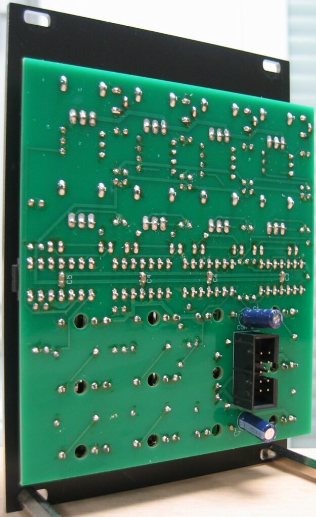
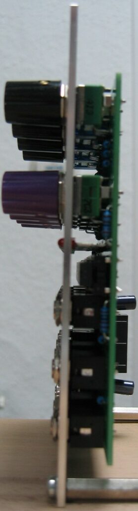
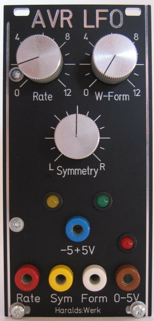
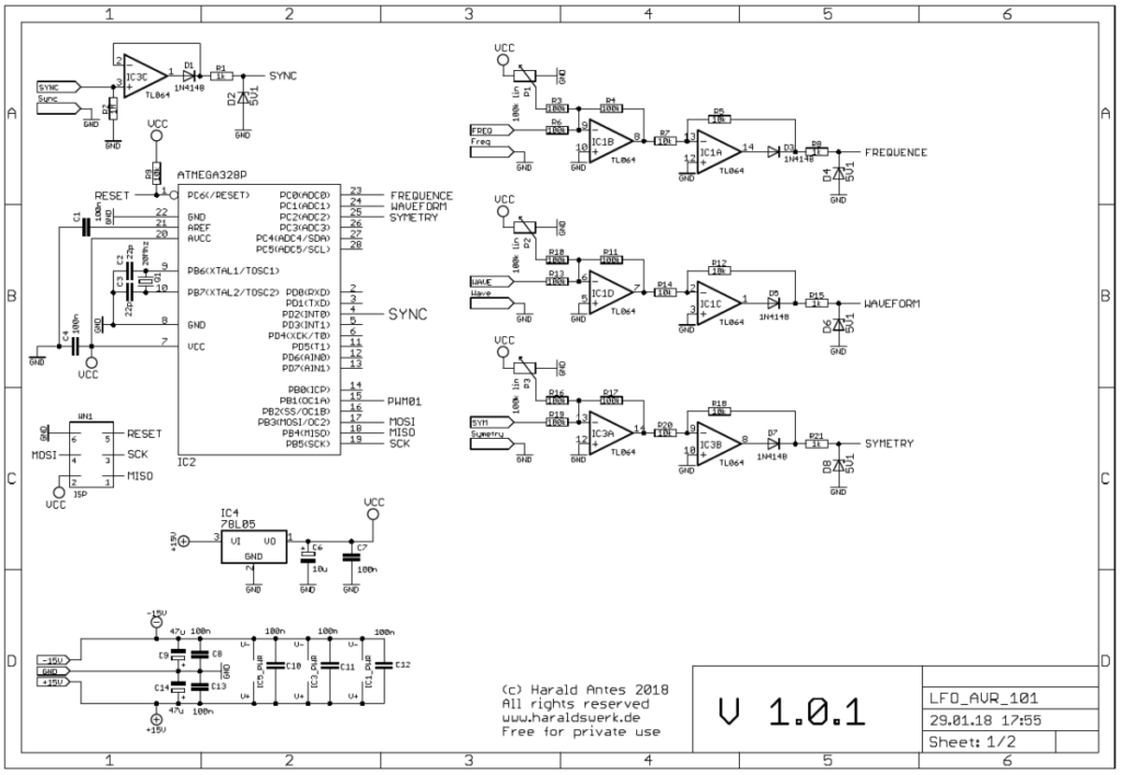
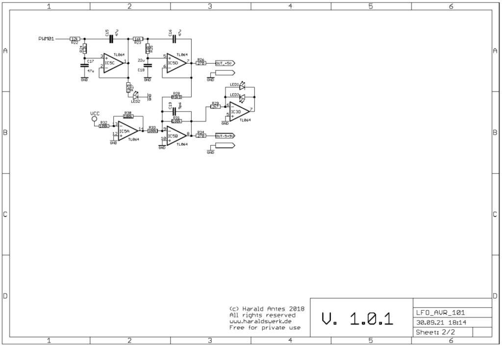
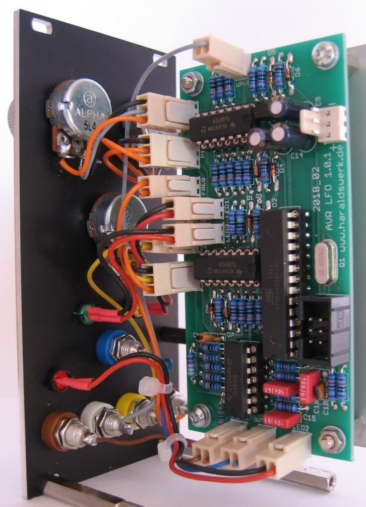
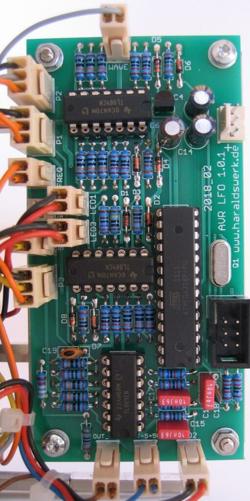
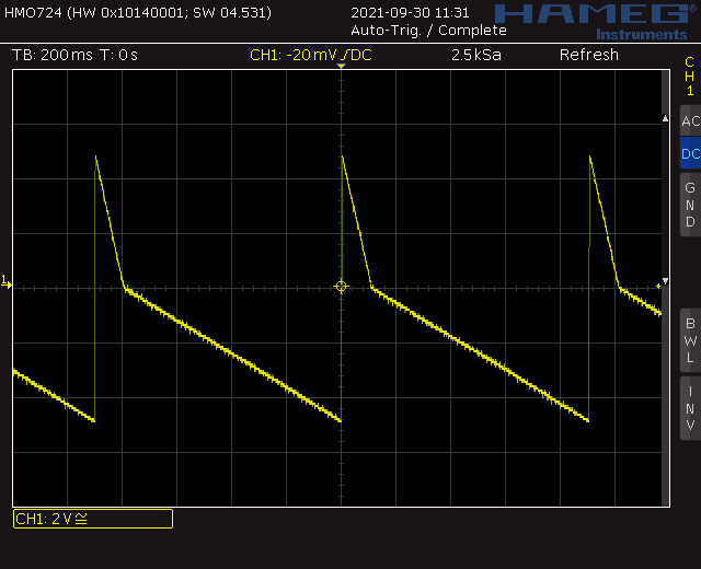
This is an old project dated back to December 2017. It was intended to learn some basics about the hard- and software of the ATMEGA series from AVR. It is kept simple. Just three analog inputs, one interrupt input and PWM output with filter are used. It is up to you what software you want to run on it. Here I made a simple voltage controlled VCO with variable symmetry. Speed, waveform and symmetry are voltage controlled. So you can change the triangle from ramp up to triangle to ramp down. Or make one halve of the sine very small. See screenshots below. This software was mainly written to test the hardware. To my surprise it worked sufficiently well for a LFO. So I leave it as is for the moment. No fancy accumulation with fixed point arithmetic and increment interpolation. Of course there is a lot room for improving the software. I know.
Specs and features
Voltage control for speed, waveform, symmetry
Bipolar and unipolar output
Square, triangle, sine, ramp up, ramp down waveform
20MHz crystal
19.5kHz PWM 10bit resolution
Runs on +/-15V and +/-12V
Power consumption around 30mA positive, 5mA negative rail
The documentation and the Gerber files for download can be found in my website.
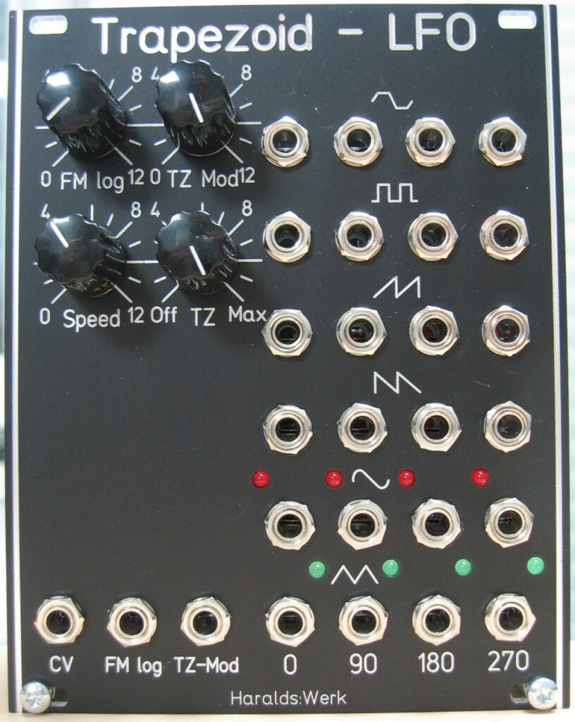
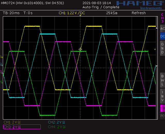
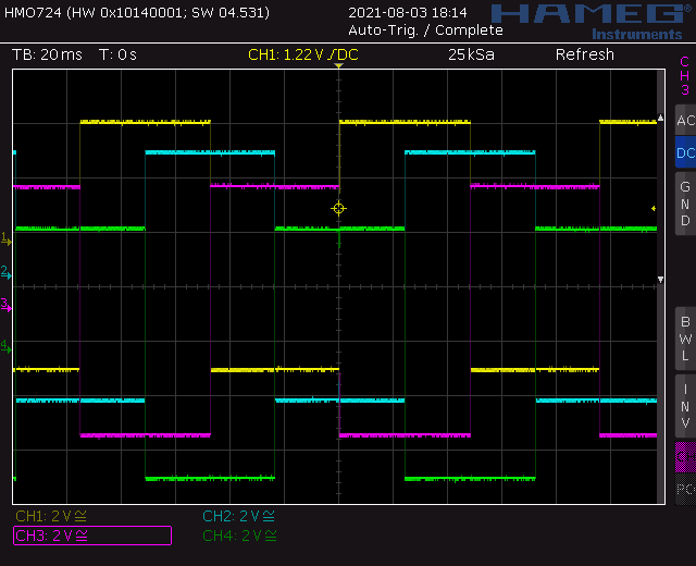
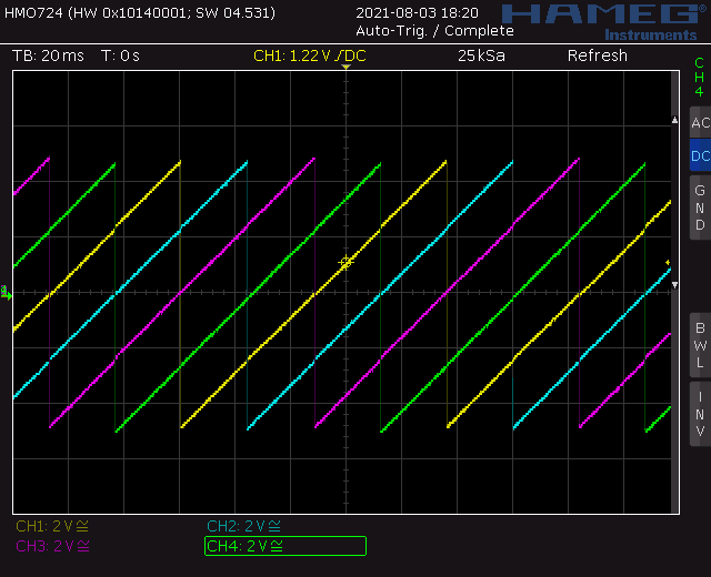
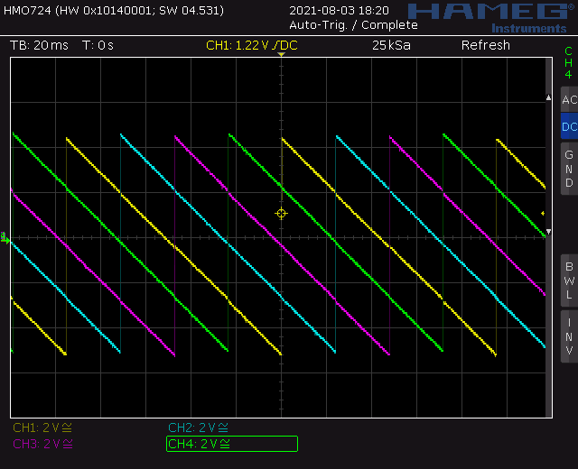
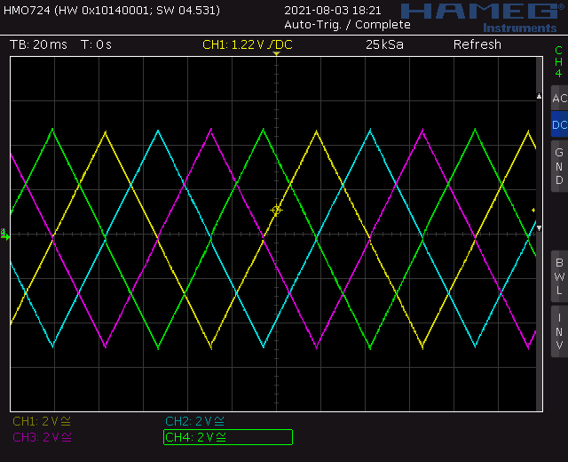
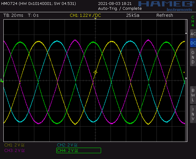
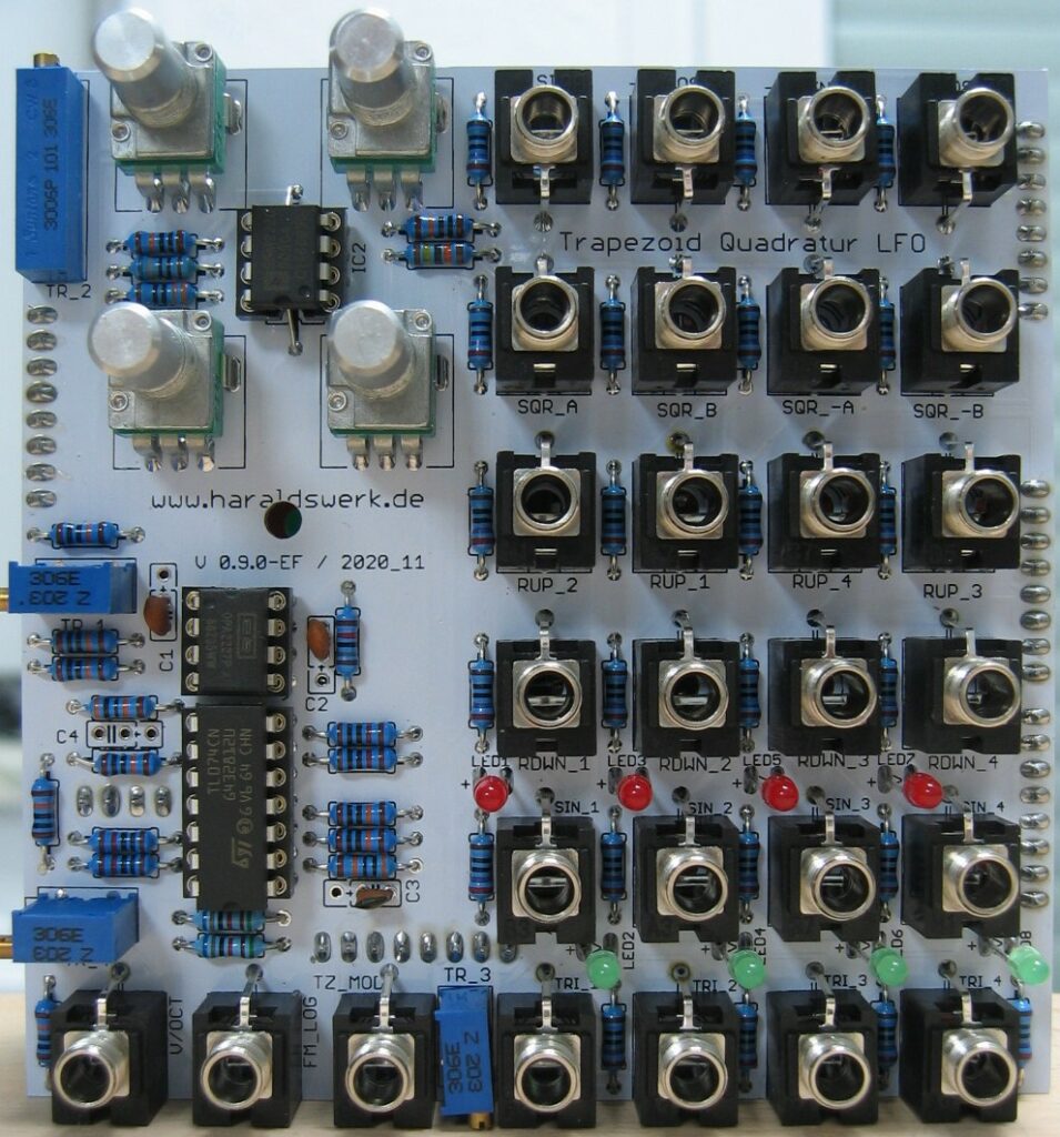
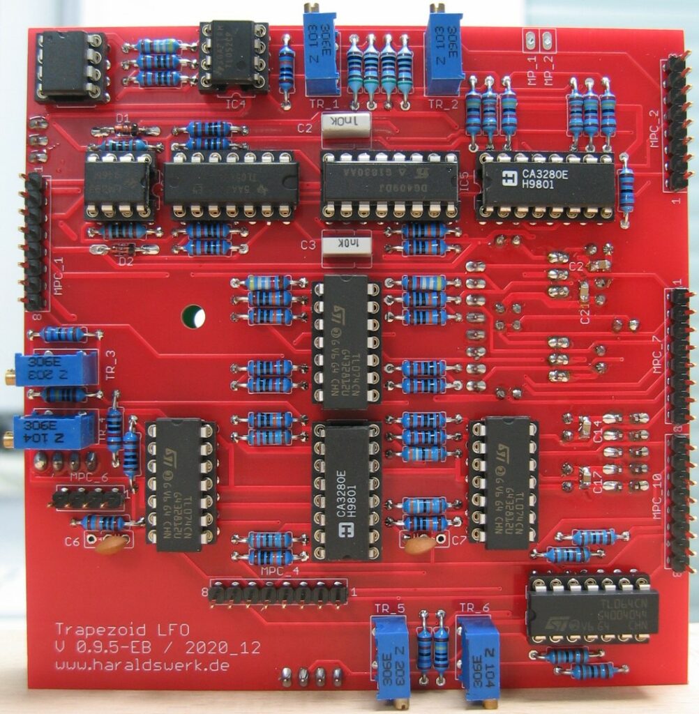
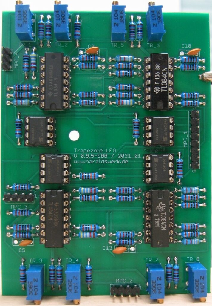
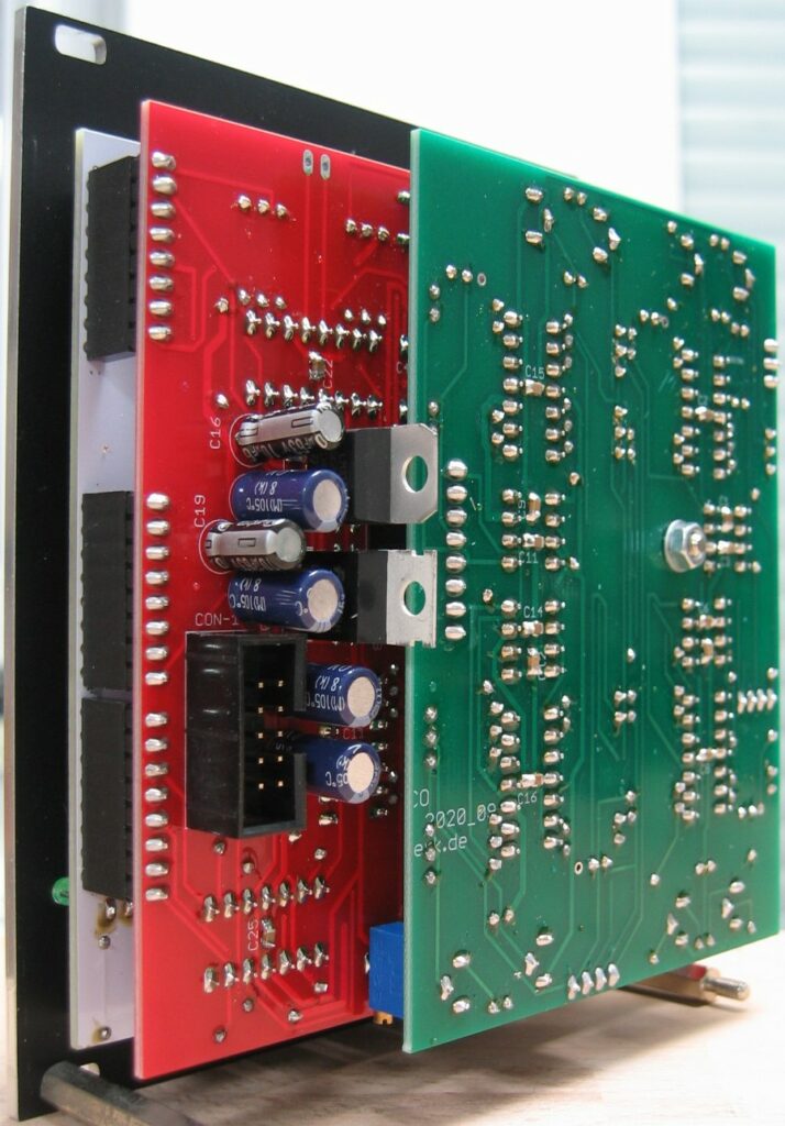
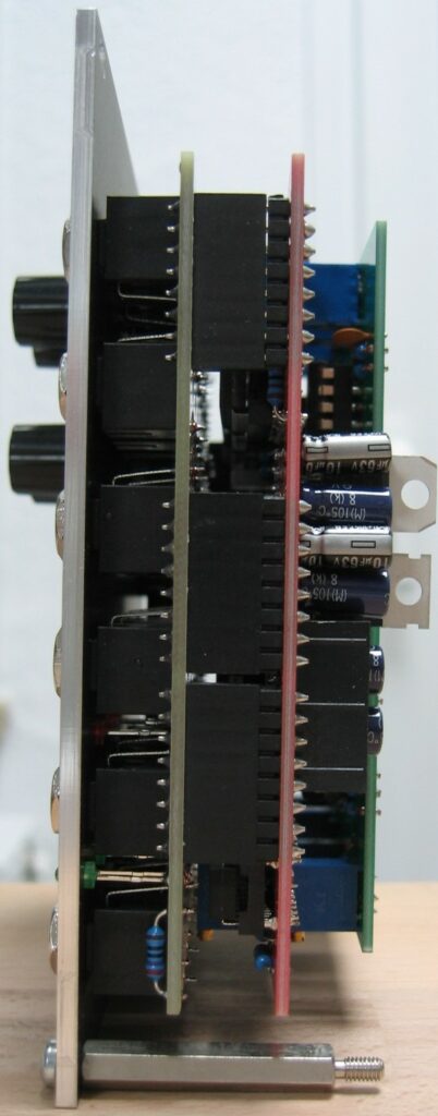
This is my Trapezoid quadrature through zero LFO. Derived from my Trapezoid quadrature through zero VCO. Still using the trapezoid VCO core designed by Don Tillman (used with permission). I found the original article and schematic about the Trapezoid VCO on Don Tillman’s site (Link to original article from 19 July 2003). The article consists off three parts with the core implementation in part 2. I kept the basic idea and changed nearly everything else. I use an other exponentiator scheme and temperature stabilization. Another reference voltage device is used. And quadrature square outputs are implemented. As well as the additional waveforms triangle, sine, ramp up and ramp down. For the LFO I made a few changes. I removed the pulse output and added the missing ramp up and ram down outputs for 180deg and 270deg. Everything else is kept the same as in my Quadrature VCO. This LFO runs from zero Hertz way up in the audio range.
Specs and features
Runs from zero Hertz to audio range.
Trapezoid quadrature output
Square quadrature output
Triangle quadrature output
Sine quadrature output
Ramp up quadrature output
Ramp down quadrature output
Through zero modulation
V/Oct, FM log and trough zero CV input
Temperature compensated
Runs on +/-15V and +/-12V
Power consumption around 110mA each rail
The documentation and the Gerber files for download can be found in my website.
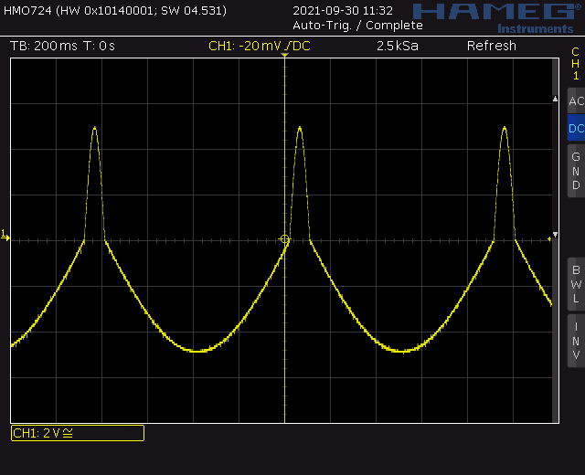
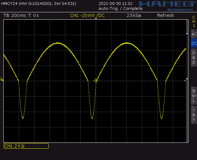
Trapezoid quadrature through zero LFO: Trapezoid quadrature outputTrapezoid quadrature through zero LFO: Trapezoid square outputTrapezoid quadrature through zero LFO: Trapezoid ramp up outputTrapezoid quadrature through zero LFO: Trapezoid ramp down outputTrapezoid quadrature through zero LFO: Trapezoid triangle outputTrapezoid quadrature through zero LFO: Trapezoid sine outputTrapezoid quadrature through zero LFO: Populated control boardTrapezoid quadrature through zero LFO: Populated main board 01Trapezoid quadrature through zero LFO: Populated main board 02Trapezoid quadrature through zero LFO: Back viewTrapezoid quadrature through zero LFO: Side view
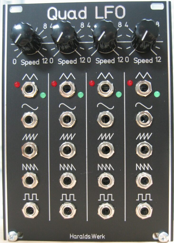
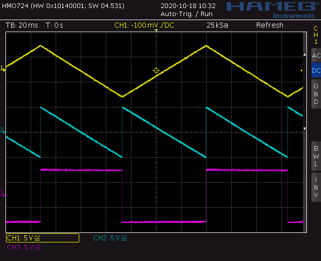
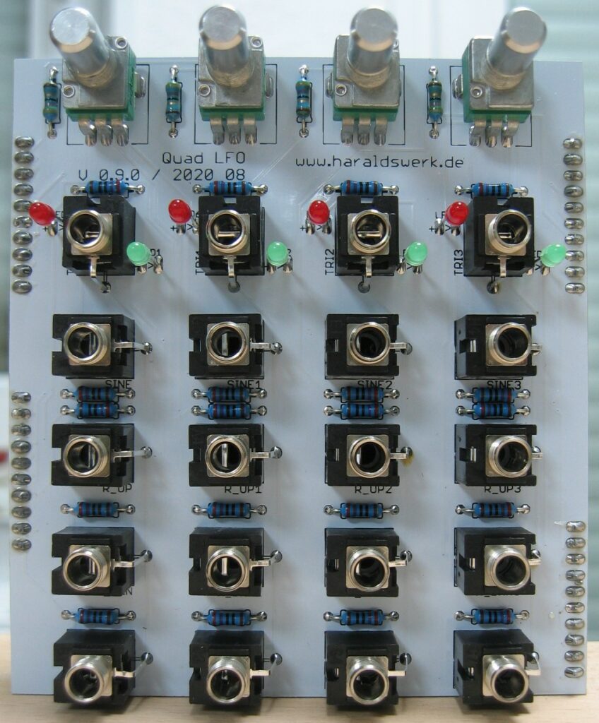
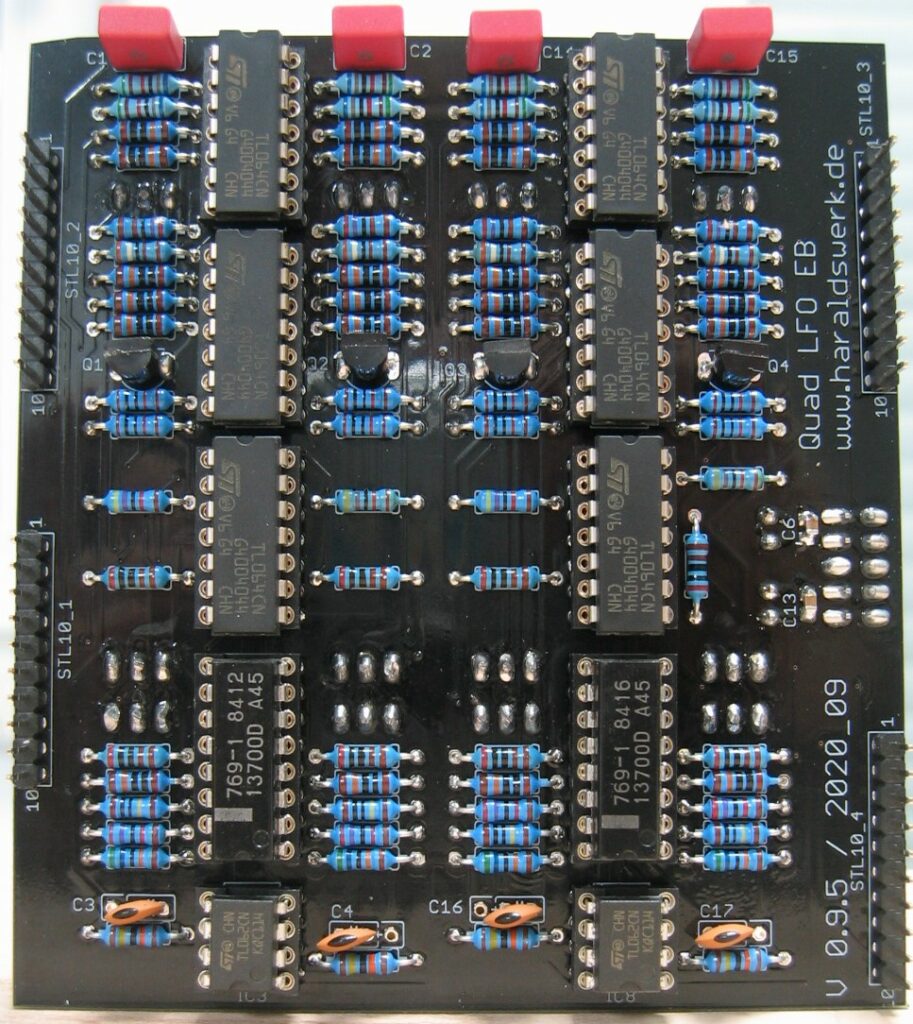
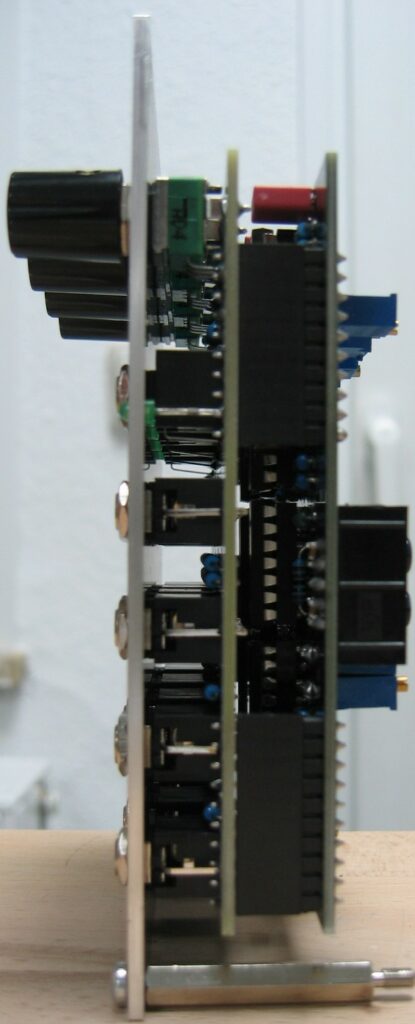
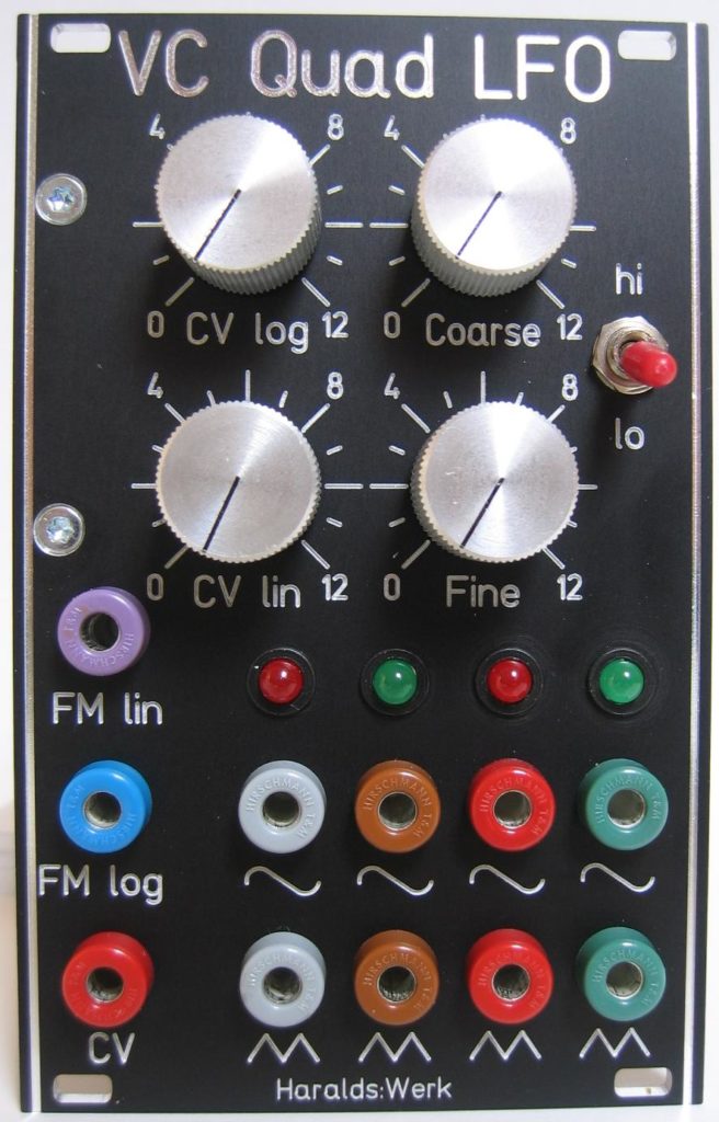
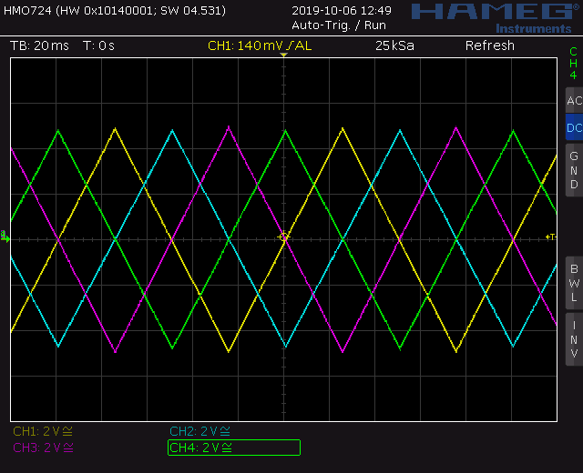
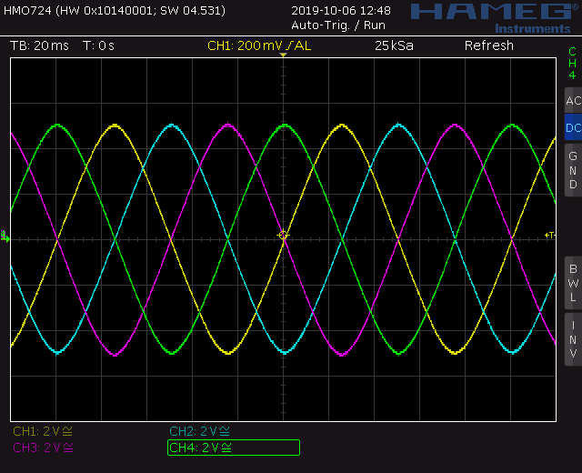
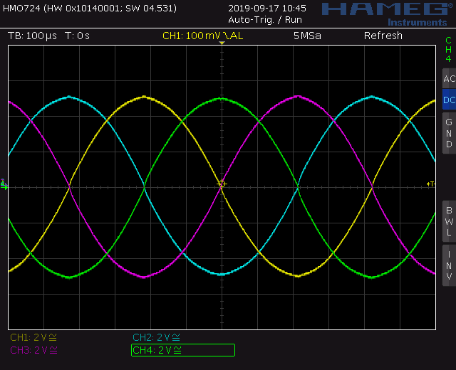
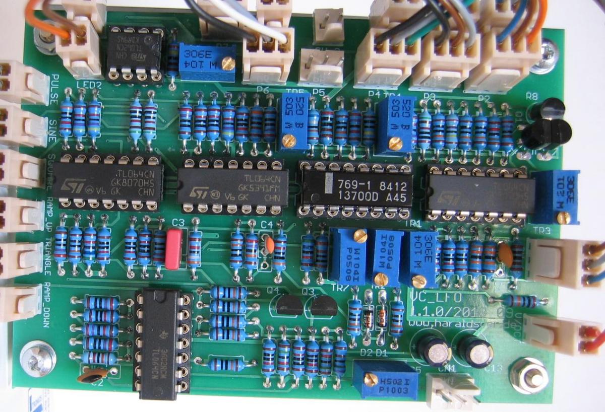
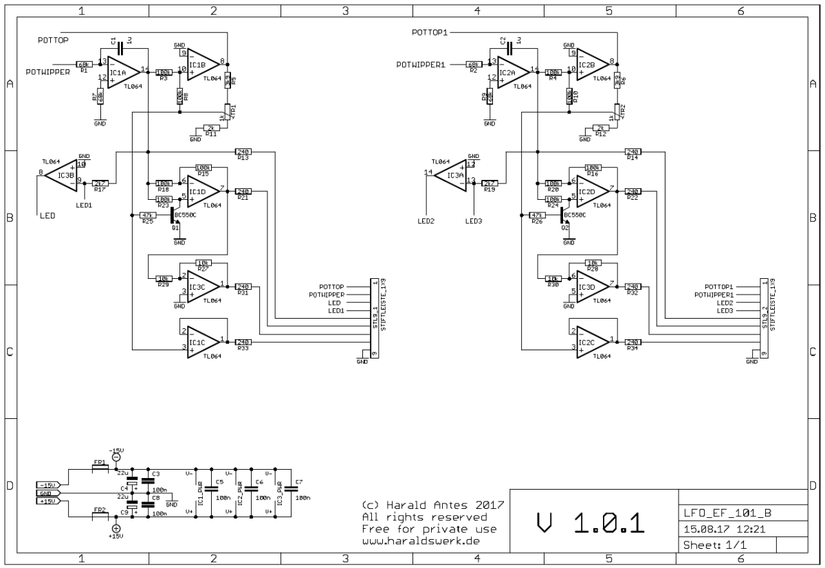
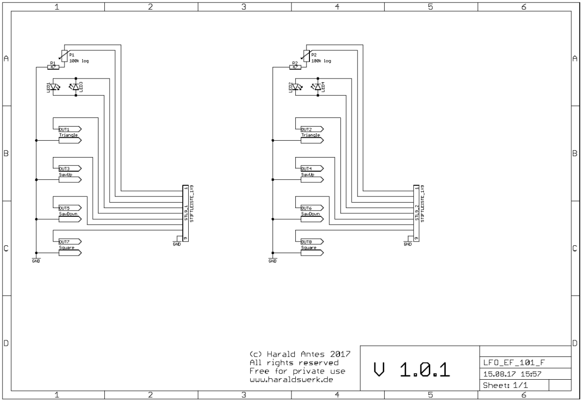
Four independent LFO with triangle, sine, ramp up, ramp down and square wave output. Output voltage 10Vpp. The sine is inverted against the triangle. Ramp up and ramp down are twice the frequency of the triangle.
Specs and features
Four independent LFO
Triangle, sine, ramp up, ramp down and square wave output
Output -5V to +5V (10Vpp)
Runs on +/-12V
Power consumption below 25mA each rail
The documentation and the Gerber files for download can be found in my website
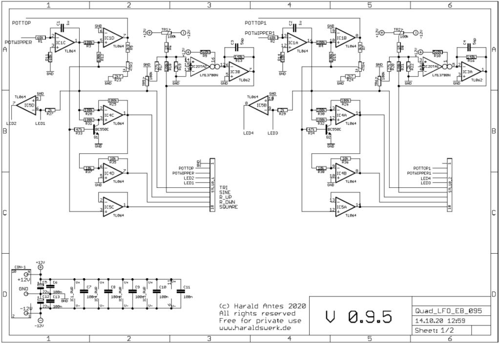
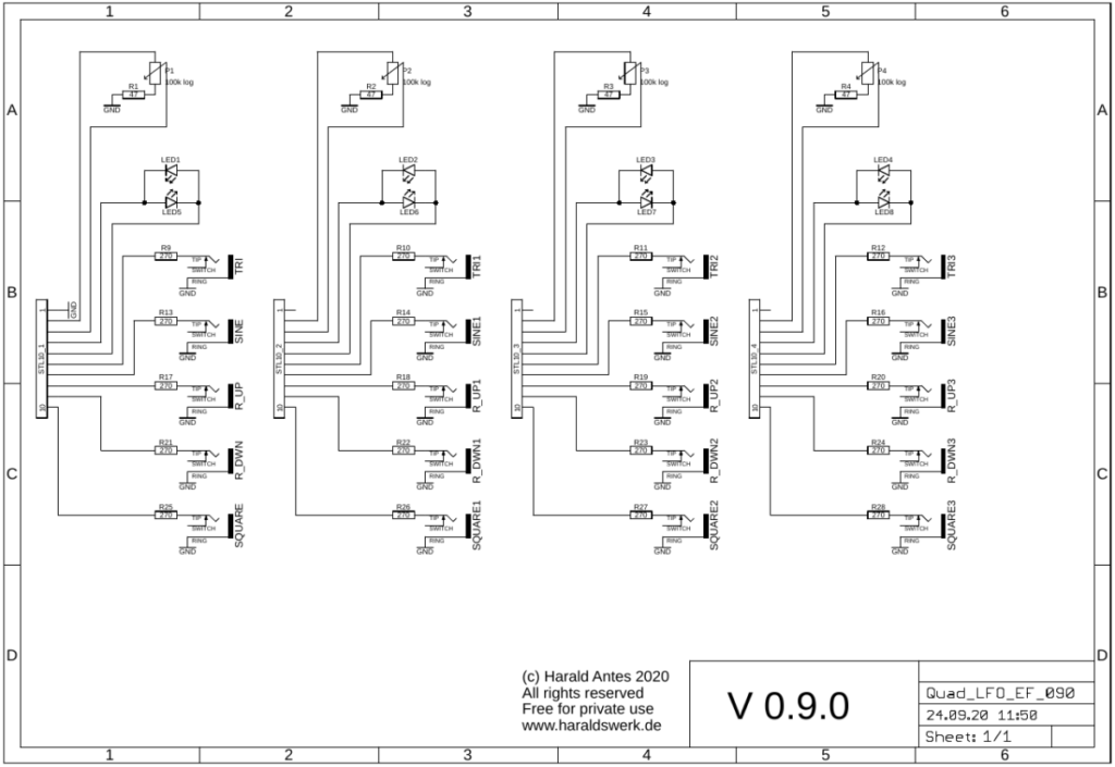
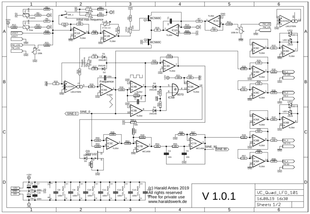
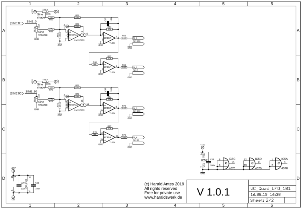
Quad LFO schematic
.Given for the first LFO. The oscillator consists of an integrator IC1C and an OpAmp Schmitt-Trigger IC1D. The triangle wave of the oscillator arises through the feedback of the trigger output to the input of the integrator. At the integrator output IC1C arises a triangle with the amplitude of the hysteresis of the Schmitt-Trigger. The input voltage of the integrator sets the rise and fall time of the voltage output. The square wave output is buffered with IC5C. The circuitry around IC4C provides the saw output. IC4D inverts the saw. The sine shaper is build with the OTA IC2OTA2 and IC3B. IC5D drives the LED.
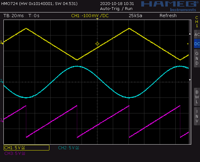
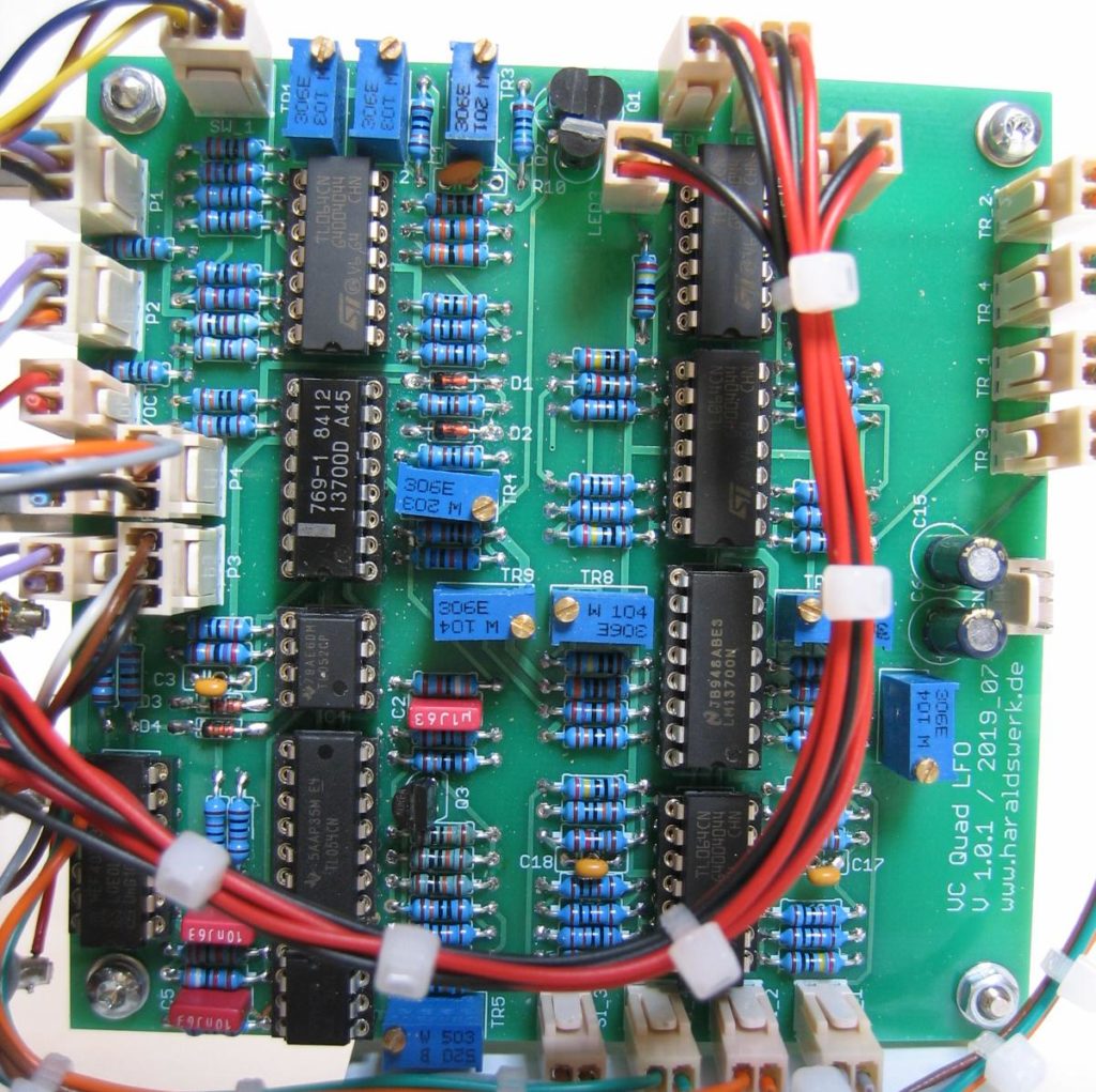
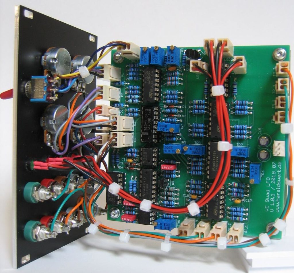
Quad LFO schematicQuad LFO waveforms screenshotQuad LFO waveforms screenshotQuad LFO populated control PCBQuad LFO populated main PCBQuad LFO side view
I want
to rotate sound through four channels of my modular synthesizer. Or
move successive through different CV or audio sources. This is easily
achieved with a quadrature LFO and four VCA. The core of this voltage
controlled quadrature LFO was published in Electronotes EN#122 pg13ff
1981 and designed by Thomas Henry. I took the core and added the
voltage control and the sine shapers.
The
voltage control part and the sine shaper are well known designs. The
triangle core is commonly used as well. The interesting part is how
the 90° triangle is derived. The Electronotes EN#122 gives a very
detailed description what is going on.
Voltage controlled quadrature LFO populated PCBVoltage controlled quadrature LFO triangle output screenshotVoltage controlled quadrature LFO sine output screenshotVoltage controlled quadrature LFO back view
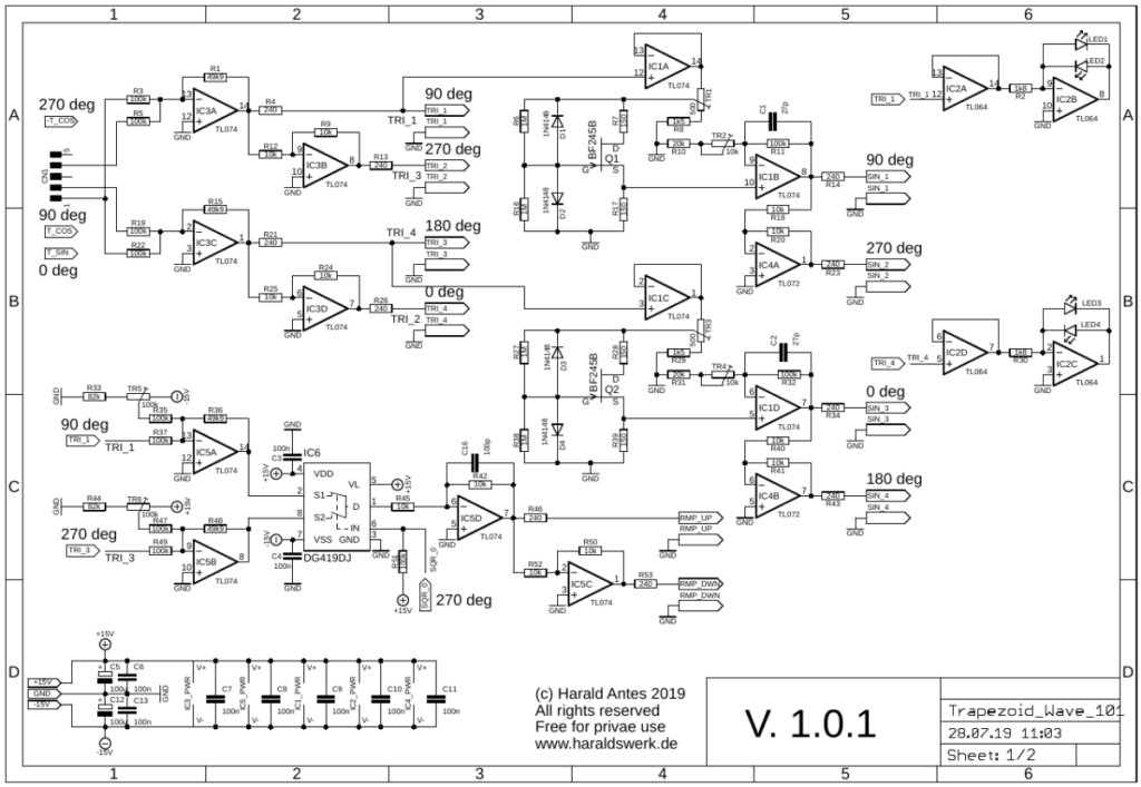
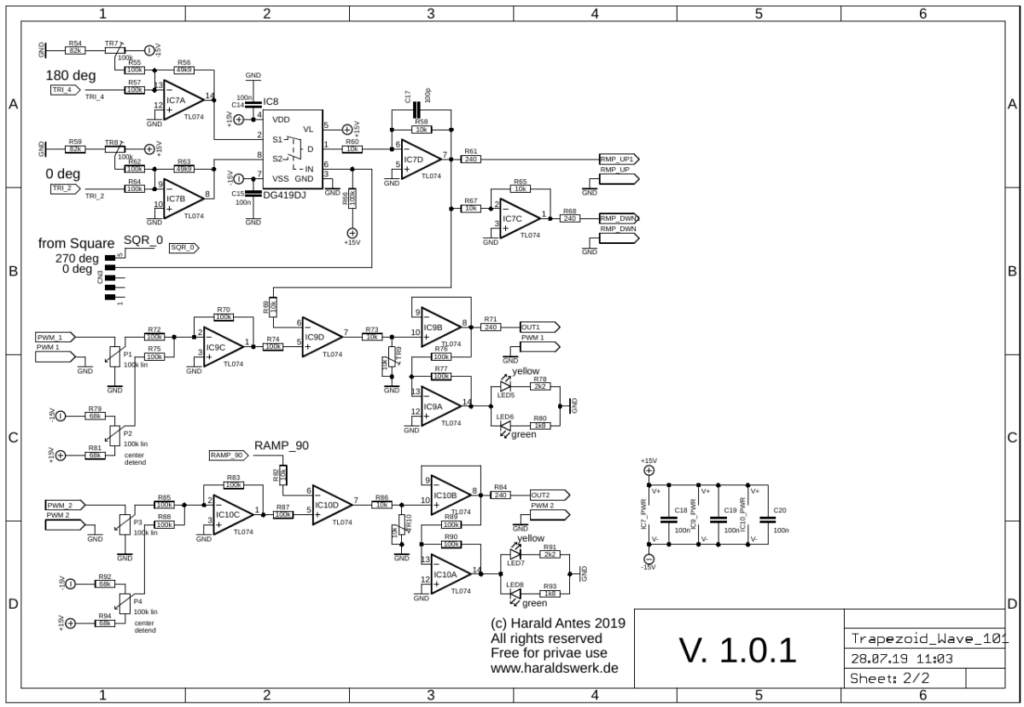
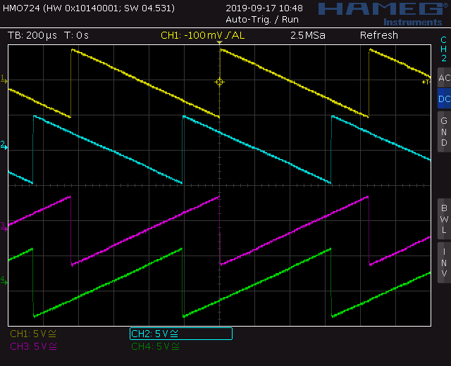
This is the waveshaper for my Trapezoid quadrature through zero VCO. It gives the quadrature outputs for triangle, sine and the outputs for saw (ramp up, ramp down) and pulse. To use it you need my Trapezoid quadrature VCO. The waveshaper has no external input for waves, it is internally connected with the Trapezoid quadrature VCO
Schematic 01 quad waveshaper for quadrature thru zero VCOSchematic 02 quad waveshaper for quadrature thru zero VCO
The
triangle waves are created by algebraically averaging two trapezoid
waves 90° apart. This is done here with IC3A for 270° and 0°. IC3C
adds and averages 90° and 0°. You can use other combinations as
well. IC3B and IC3D gives the inverse triangle waves. The sines are
derived from the triangle with well known “old style”
circuitry. The ramp outputs are build from two triangles 180° apart,
level shifted and switched between them with the square wave. IC5A
takes the 90° triangle, shift it up to 0..10V and lowers the
amplitude to 0..5V. IC5B takes the 270° triangle shift it down to
0..-10V and lowers the amplitude to 0..-5V. IC6 (DG409) switches
between this two triangles with means of the 270° square. Switching
in the right moment put the needed parts of the triangle back
together to the saw. The pulse outputs are done with the usual
technique moving the switching point of a comparator around with the
ramp wave.
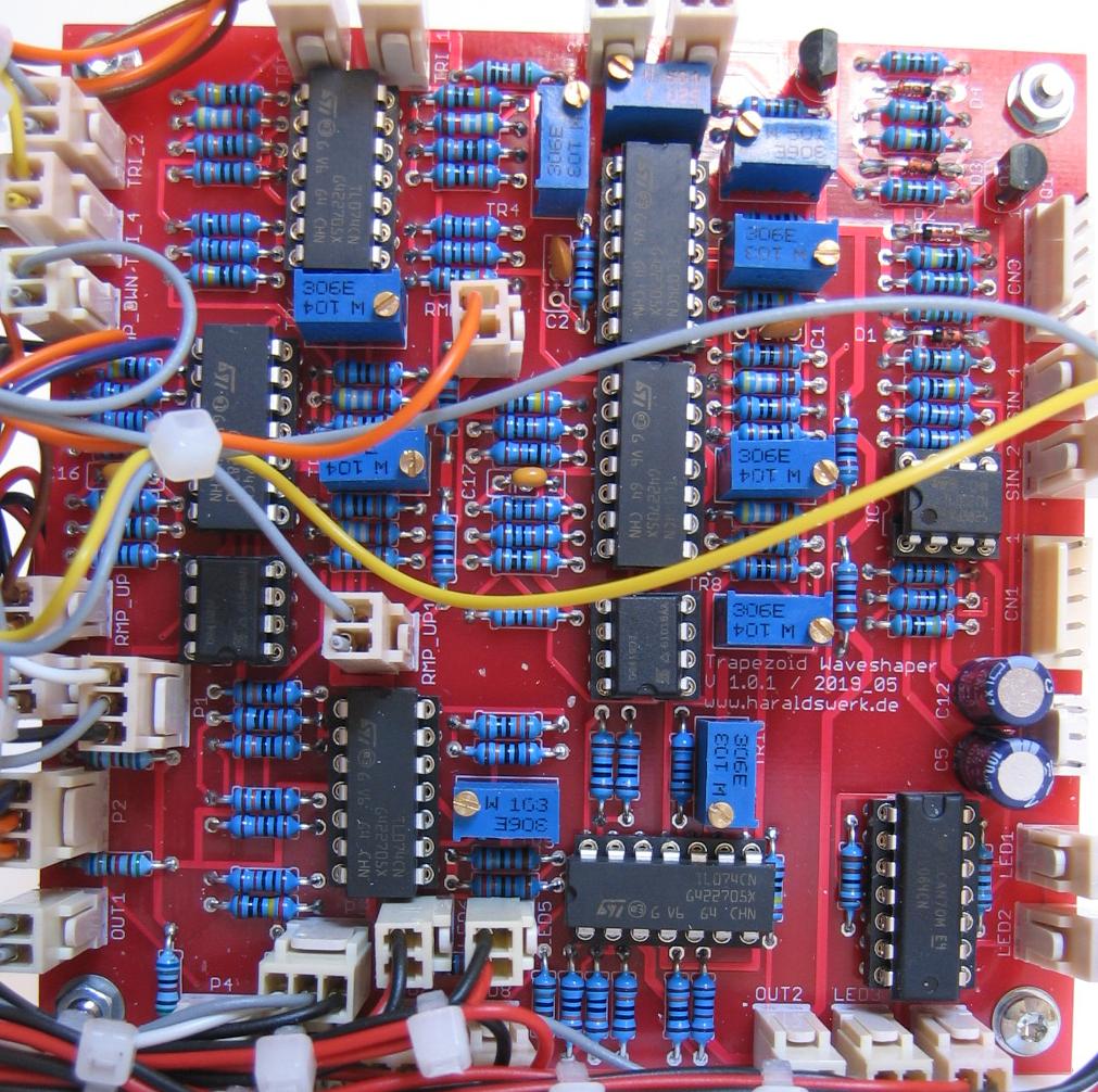
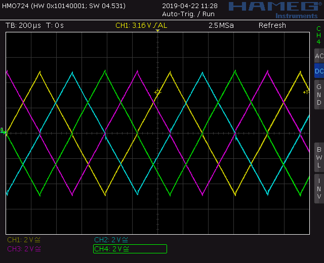
PCB quad waveshaper for quadrature thru zero VCOTriangle screenshot from quad waveshaper for quadrature thru zero VCOSine screenshot from quad waveshaper for auadrature thru zero VCOSaw screenshot from quad waveshaper for auadrature thru zero VCOPulse screenshot from quad waveshaper for auadrature thru zero VCOQuad waveshaper for auadrature thru zero VCO back view
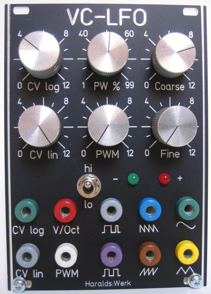
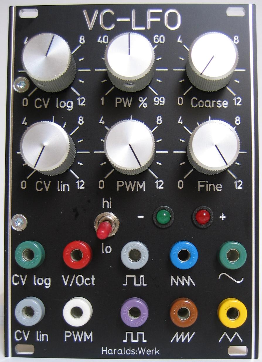
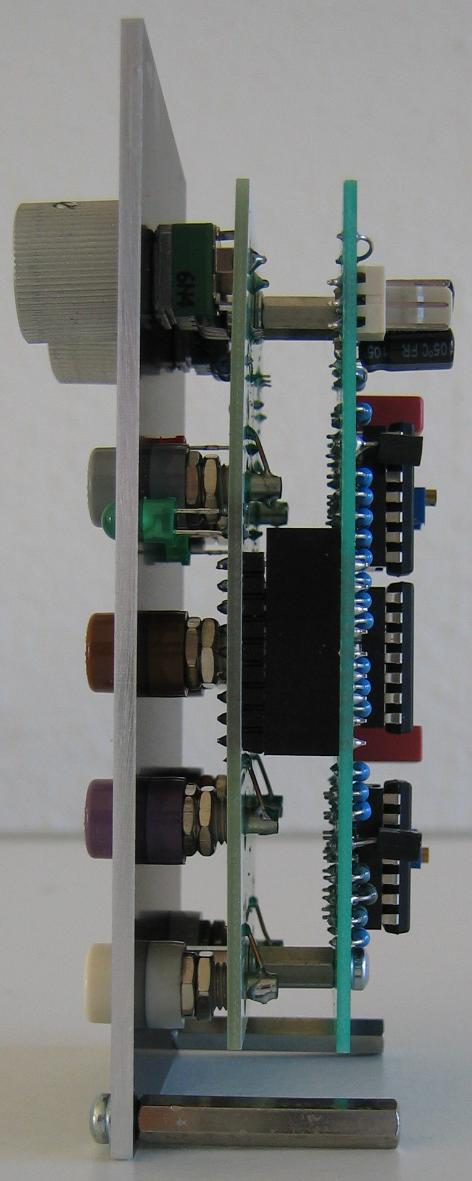
This is the flat version of my VC-LFO I’ve build this flat version to minimize the depth of the module and avoid the wiring for the potentiometers. A VC LFO with multiple synced output waveforms is a very useful and versatile module. You can’t have enough of them. They can add a lot to sounds making them more animated. This one provides triangle, ramp up, ramp down pulse. square and sine wave output (-5V to +5V). The frequency range is easily adjusted to your needs from some minute per cycle up to 700Hz. I started with the VC LFO design form Ray Wilson MFOS but changed the exponentiator and pulse adjust schematic completely. I have added a range switch and a linear FM input as well.
Specs and features
Synced triangle, ramp up, ramp
down, pulse, square and sine wave output
Output -5V to +5V
log and lin CV input
Temperature compensated
Voltage controlled pulse width
Range switch
Coarse and fine frequency setting
Runs on +/-15V and +/-12V
Power consumption below 10mA each rail
The documentation and the Gerber files for downloadcan be found in my website.
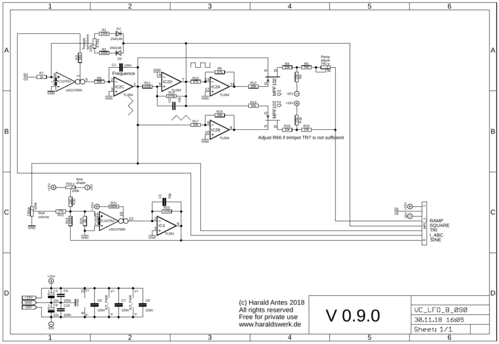
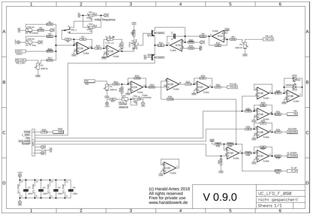
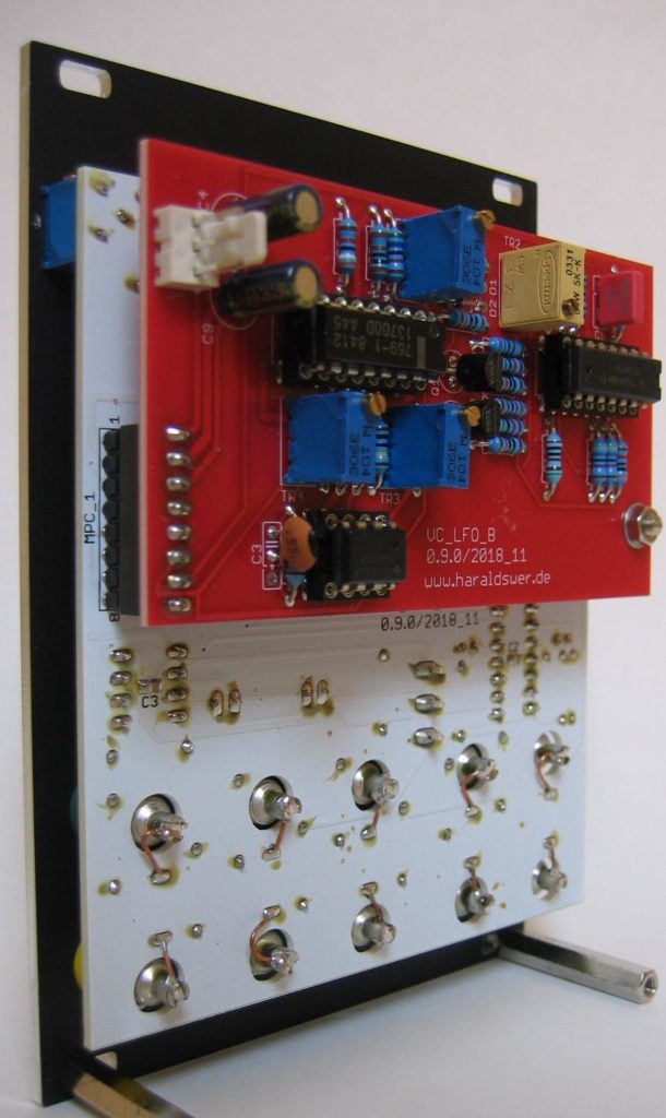
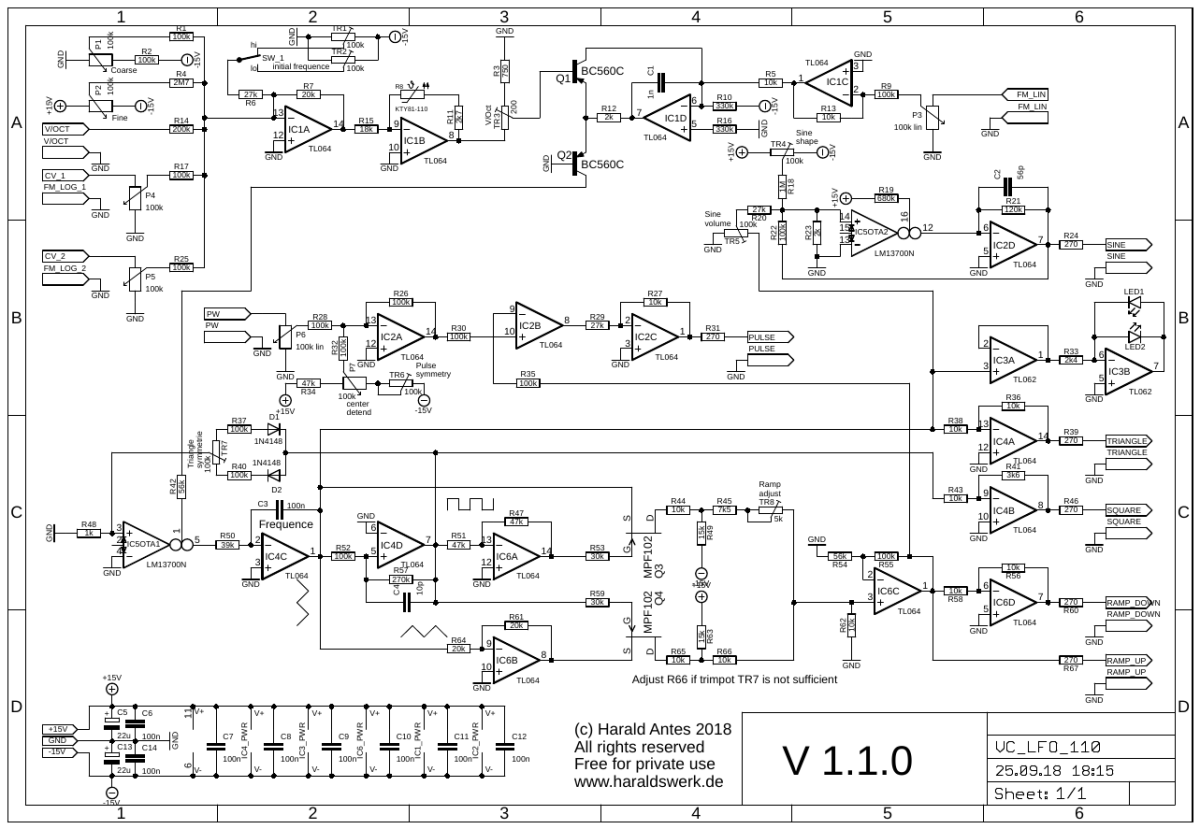
Voltage controlled LFO schematic back PCBVoltage controlled LFO front PCB
C1 and
associated components comprise a linear voltage to log current
converter. IC1A sums the control voltages. IC1B provides the temp
compensation realized with KTY81-110. TR3 adjusts the V/Oct
characteristic. Q1 and Q2 forms the log converter with IC1D as
constant current source. IC1C scales the control voltage for the
linear FM input. The transconductance of IC1OTA1 controls the
frequency of the oscillator. IC2C, C1 and associated components
comprise an integrator. When current flows into IC1OTA1 output the
integrator ramps up, when current flows out of IC1OTA1 the integrator
ramps down. When the integrators output goes above the threshold of
comparator IC2D its output goes high. The output of IC2D is fed to
the non-inverting input of IC1OTA1 OTA through D1, D2, R1, R2 and
TR1. TR1 balances the current flowing during the high and low periods
of IC2D. With TR1 you can adjust the symmetry of the triangle. While
IC2Ds output is high current flows out of IC1OTA1 OTA and the
integrator ramps down until the voltage at the input of IC2D goes low
enough to overcome the hysteresis provided by R13 and its output goes
low. When this happens the comparator starts to ramp up again and
thus we have a triangle wave at the output of IC2C. The bias of the
comparator IC2D is controlled by the current generated by the linear
voltage to log current convertor. This controls the current that
flows in and out of IC1OTA1 and thus the frequency of the oscillator.
The sawtooth is created by mixing portions of the original
triangle wave and an inverted version of the triangle wave. N-FETs Q1
and Q1 are used as analog switches.
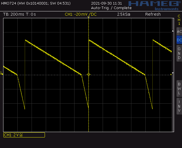
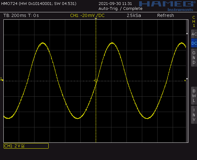
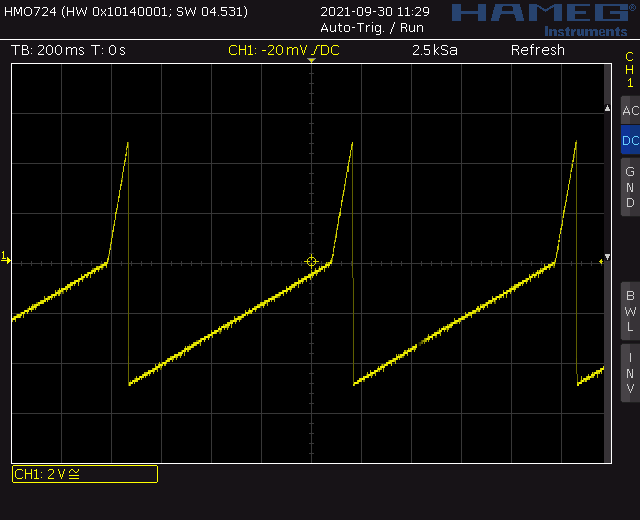
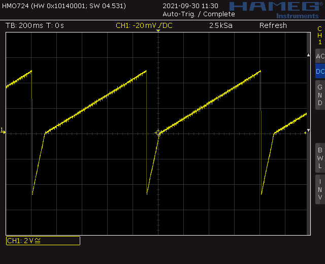
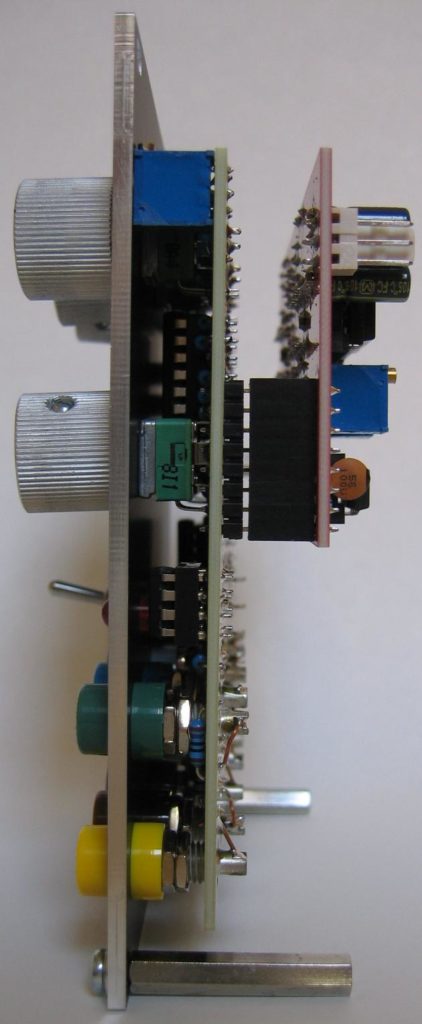
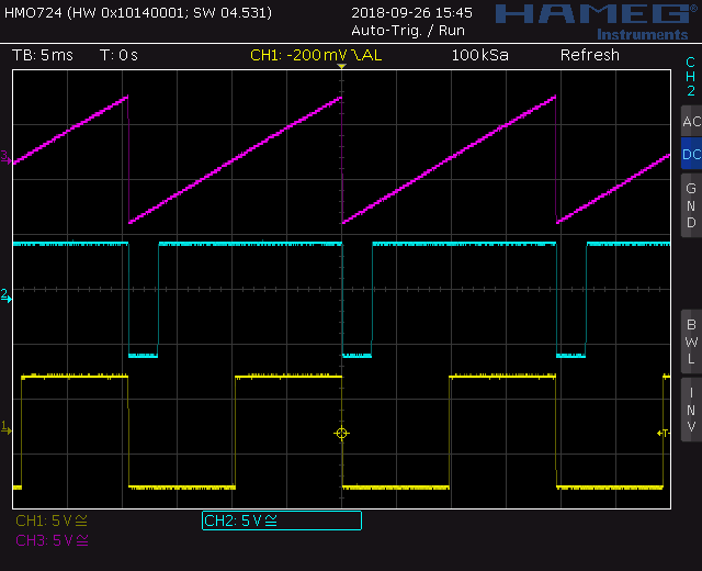
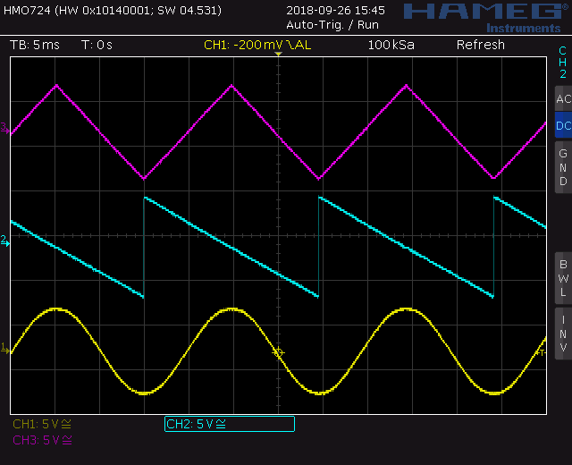
Voltage controlled LFO screenshot waveforms: ramp, pulse, squareVoltage controlled LFO screenshot waveforms: triangle ramp down, sineVoltage controlled LFO back viewVoltage controlled LFO side view
A VC LFO with multiple synced output waveforms is a very useful and versatile module. You can’t have enough of them. They can add a lot to sounds making them more animated. This one provides triangle, ramp up, ramp down pulse. square and sine wave output (-5V to +5V). The frequency range is easily adjusted to your needs from some minute per cycle up to 700Hz. I started with the VC LFO design form Ray Wilson MFOS but changed the exponentiator and pulse adjust schematic completely. I have added a range switch and a linear FM input as well.
Specs and features
• Synced triangle, ramp up, ramp down, pulse, square and sine wave output
• Output -5V to +5V
• log and lin CV input
• Voltage controlled pulse width
• Range switch
• Coarse and fine frequency setting
• Runs on +/-15V and +/-12V
• Power consumption below 10mA each rail
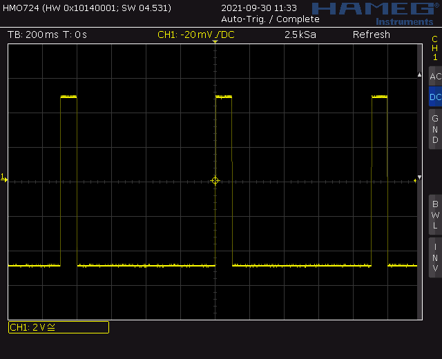
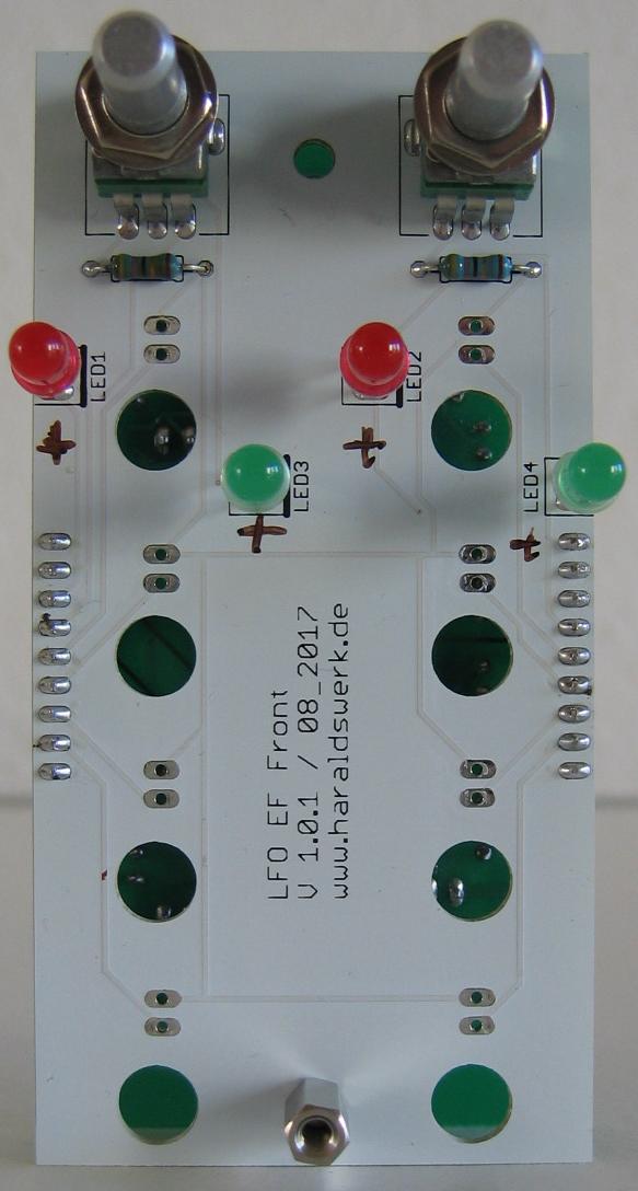
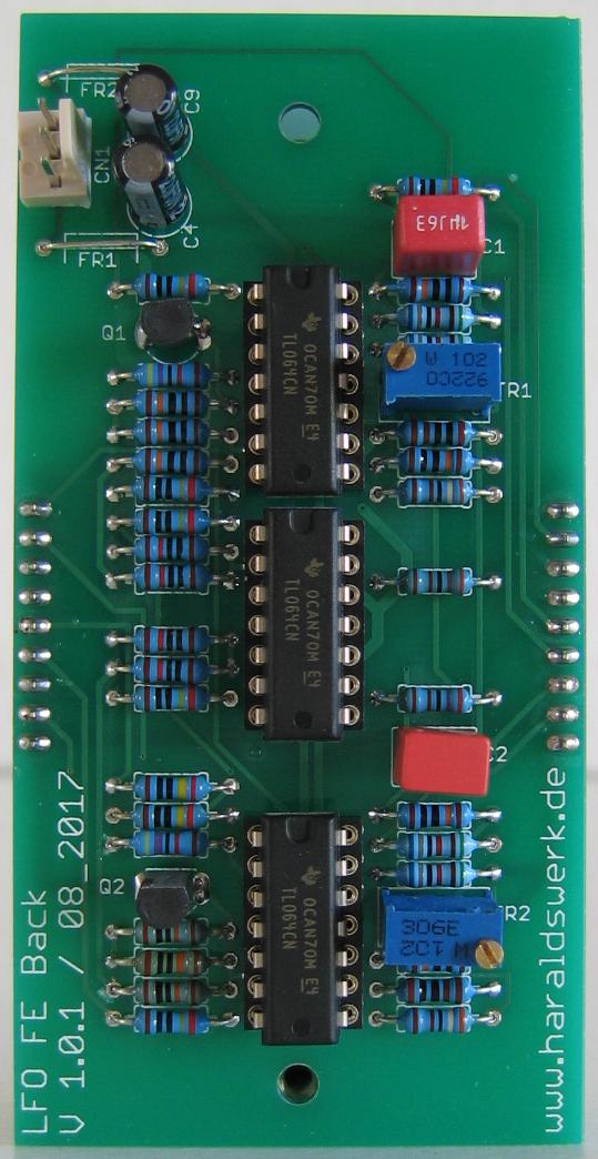
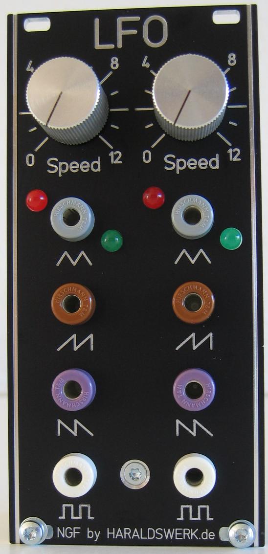
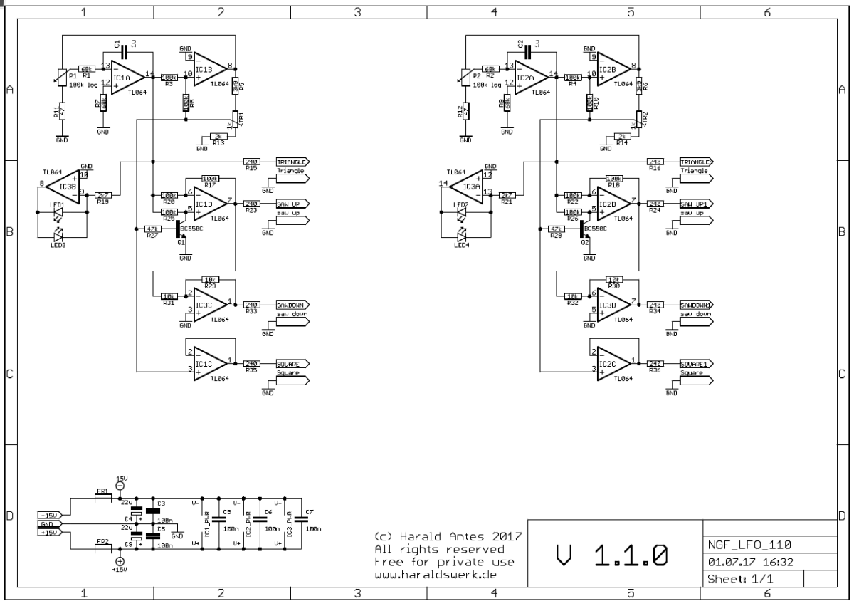
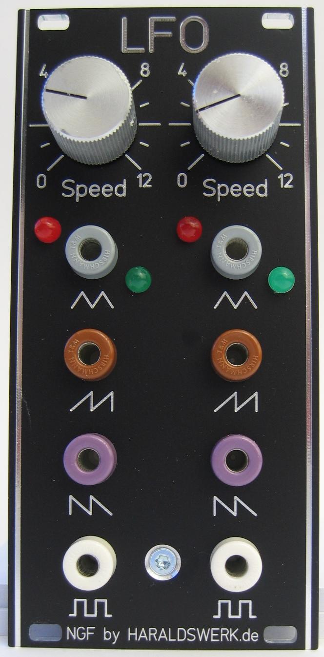
This is the LFO module for my Next Generation Formant project. It provides triangle, ramp up, ramp down and square wave output (-5V to +5V). This design follows closely the original from the Elektor Formant.
Most noticeable change is moving to a “flat” design. The depth of the module is significantly reduced and most important no more potentiometer wiring is needed!
The oscillator consists of an integrator IC1A and an OpAmp Schmitt-Trigger IC1B. The triangle wave of the oscillator arises through the feedback of the trigger output to the input of the integrator. At the integrator output IC1A arises a triangle with the amplitude of the hysteresis of the Schmitt-Trigger. The input voltage of the integrator sets the rise and fall time of the voltage output. The square wave output is buffered with IC1C. The circuitry around IC1D provides the saw output. IC3C inverts the saw.
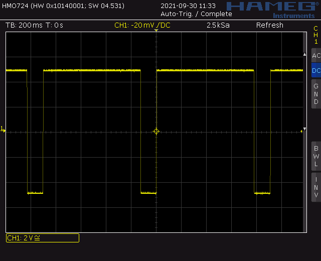
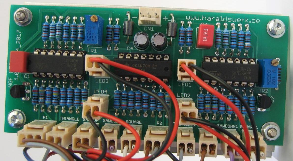
Here is the LFO module for my NGF-E project. It provides triangle, ramp up, ramp down and square wave output (-5V to +5V) This design follows closely the original from the Elektor Formant.
The oscillator consists of an integrator IC1A and an OpAmp Schmitt-Trigger IC1B. The triangle wave of the oscillator arises through the feedback of the trigger output to the input of the integrator. At the integrator output IC1A arises a triangle with the amplitude of the hysteresis of the Schmitt-Trigger. The input voltage of the integrator sets the rise and fall time of the voltage output. The square wave output is buffered with IC1C. The circuitry around IC1D provides the saw output. IC3C inverts the saw.