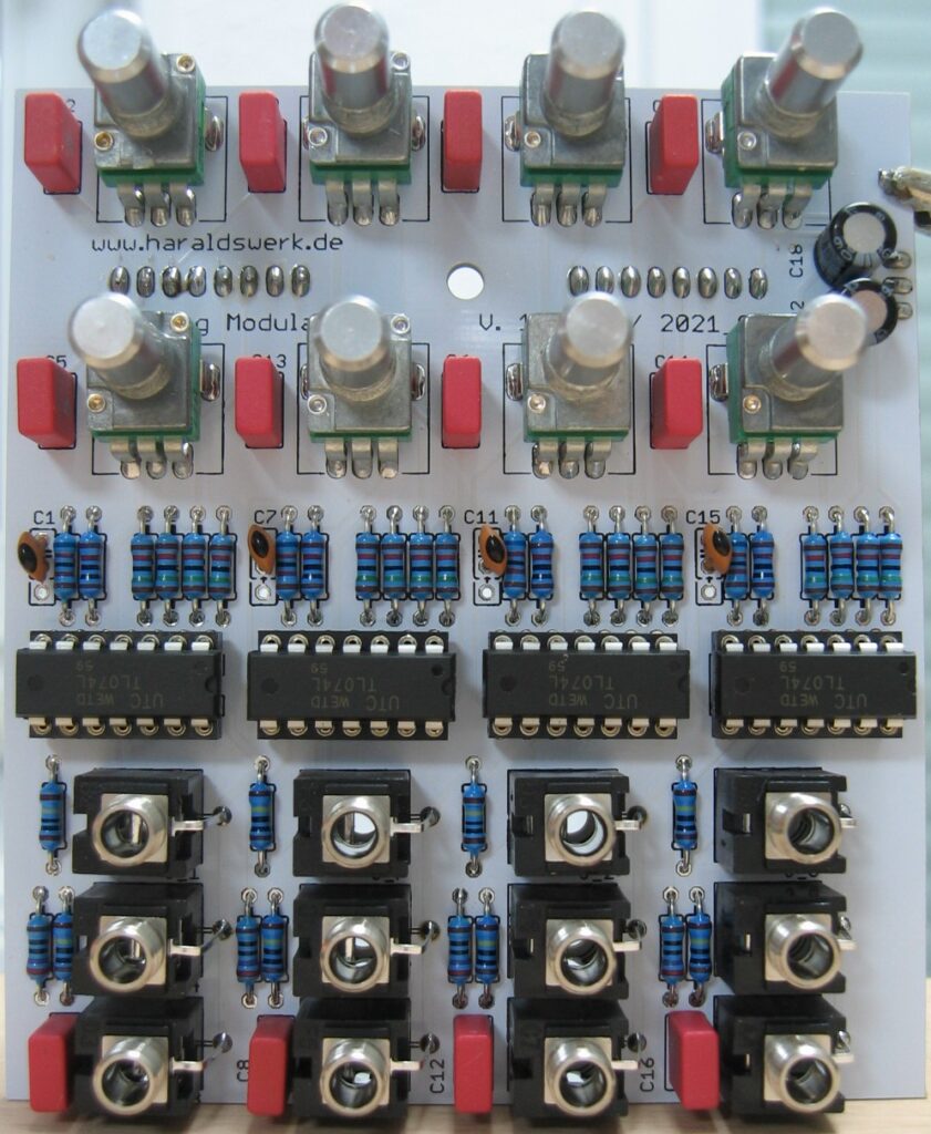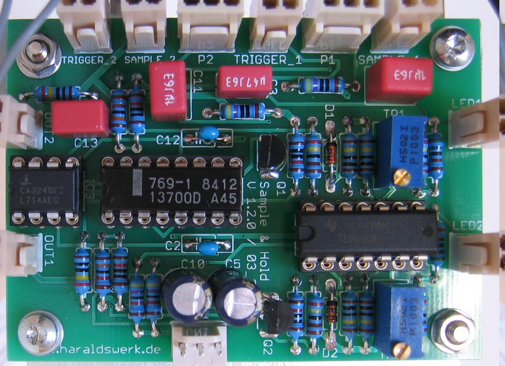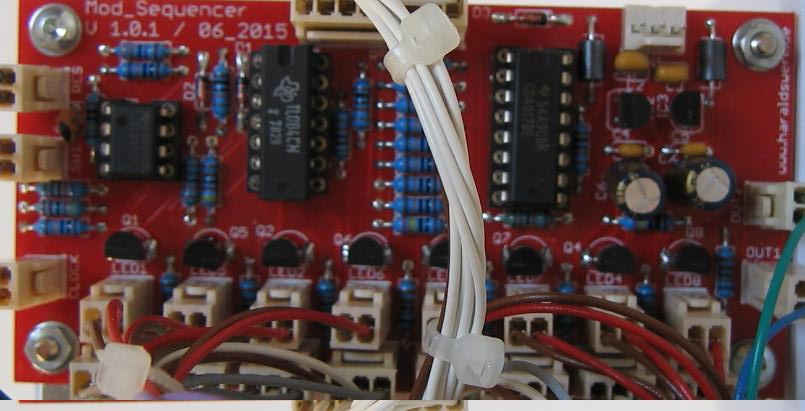
Modulation Sequencer populated PCB
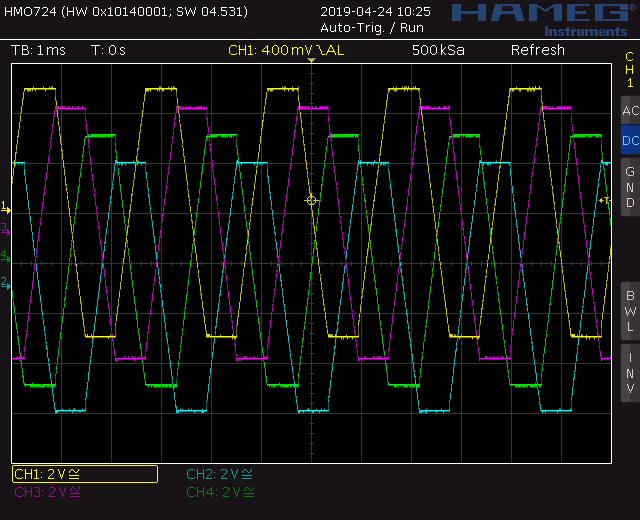
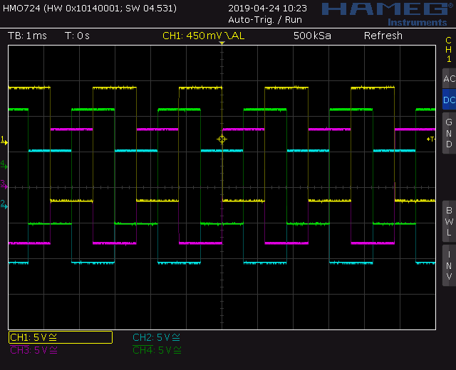
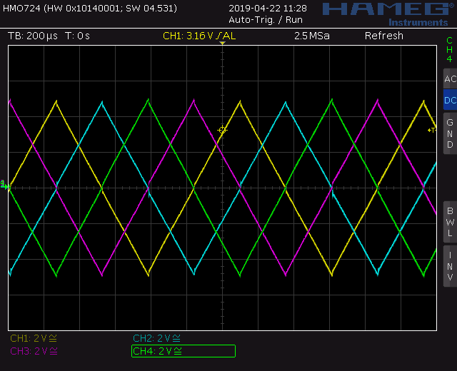
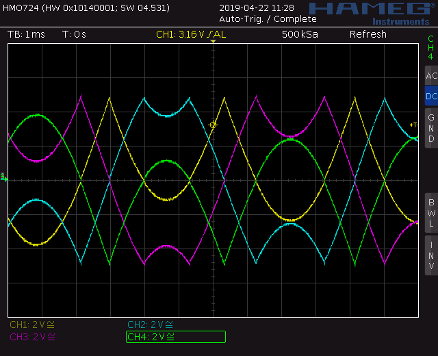
This is a small easy to use and easy to build sequencer. The sequence is adjustable from 2 to 8 steps. The output range is switchable from 0..1V to 0..5V. So you can cover 1 or 5 octaves. The sequencer is clocked from an external source. The clock range goes from very slow (LFO) to way above the audio range. When used in the audio range you can realize quite interesting envelope patterns. With the reset input you can start and reset the sequence. This is useful for creating a gated repeating pattern. Many more applications are possible.
Specs and features
2..8 steps
Switchable output 0..1V, 0..5V
Clock input
Reset input
Positive and negative output
Runs on +/-15V and +/-12V (with minor changes)
Power consumption below 10mA each rail
The documentation for download can be found in my website.
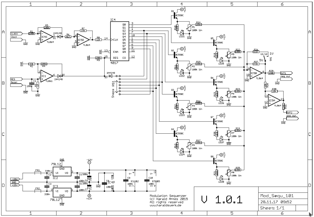
Modulation Sequencer schematic
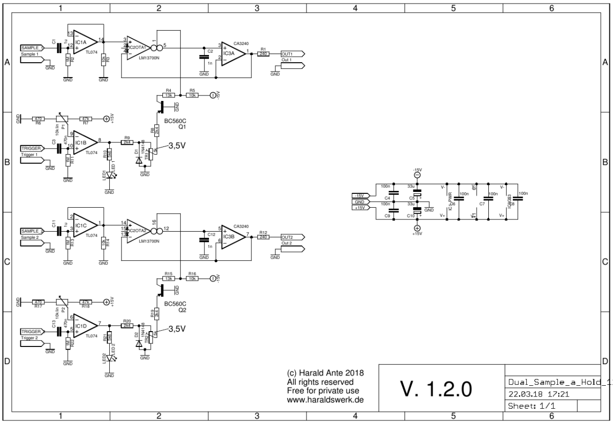
The sequencer is build around the decimal counter 4017. The clock and reset input needs at least 1/2 off the positive supply voltage to trigger. Therefore the inputs are amplified (IC5C, IC5D, IC1) so you can run the sequencer with lower input voltages. The input circuitry also protects against negative input voltages which are not allowed for the 4017. With the rotary switch you can select the length of the sequence. The rotary switch selects the output which is feed to the reset input of the 4017. The outputs are buffered with the transistors Q1 ..Q8. The emitters are connected to potentiometers which adjust the output voltage. The transistors are driving the LED for the step display as well. The output is buffered with the operational amplifier IC5B. IC5A provides the negative output.
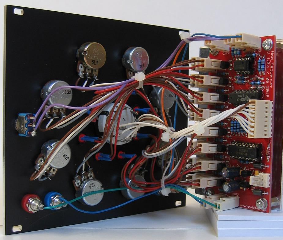
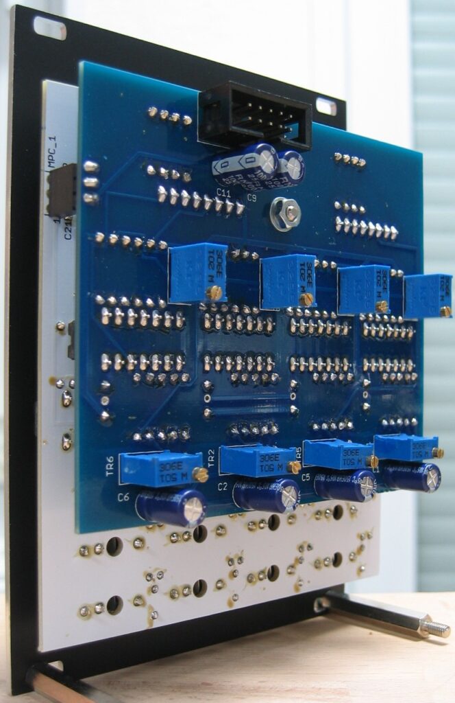
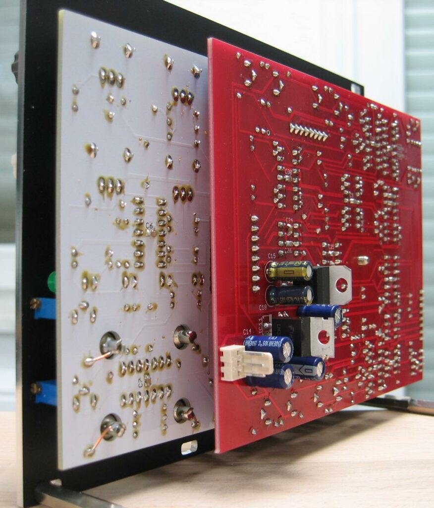
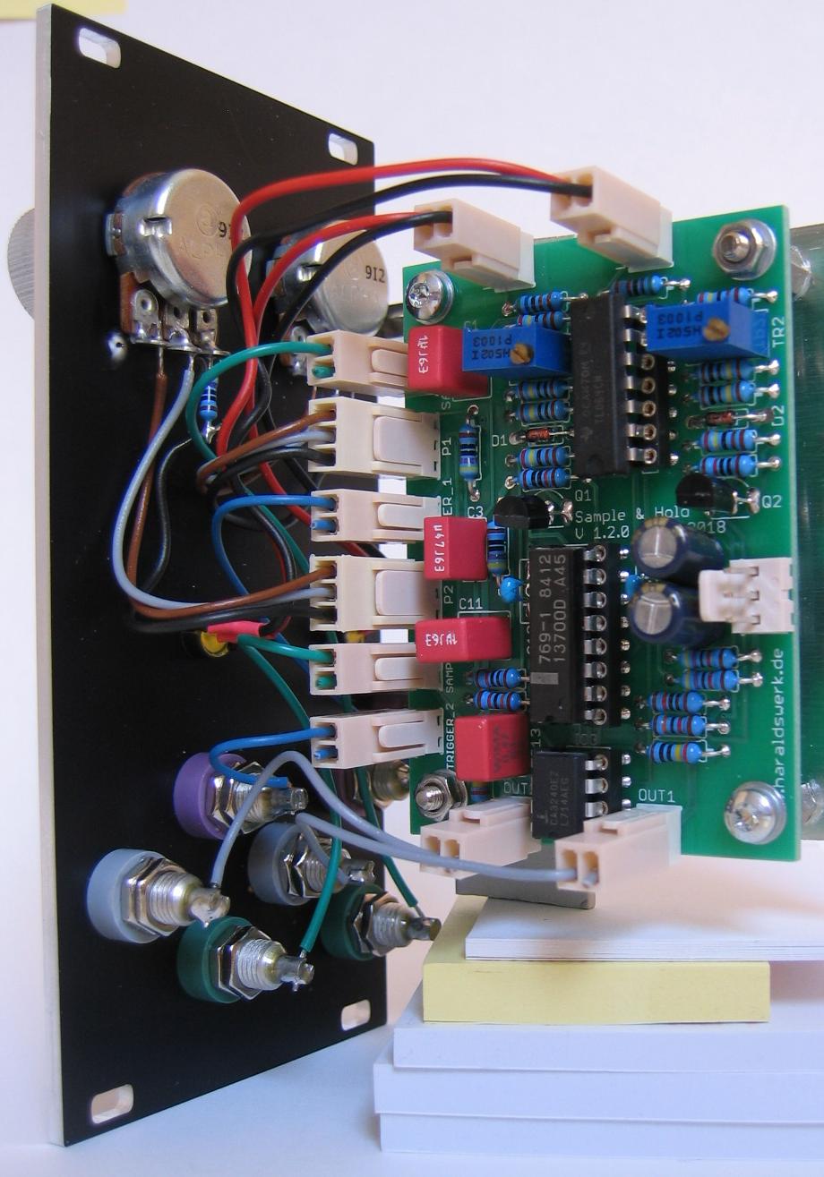
Modulation Sequencer back view
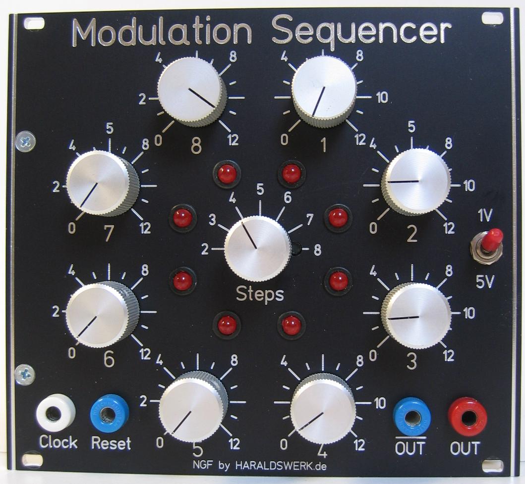
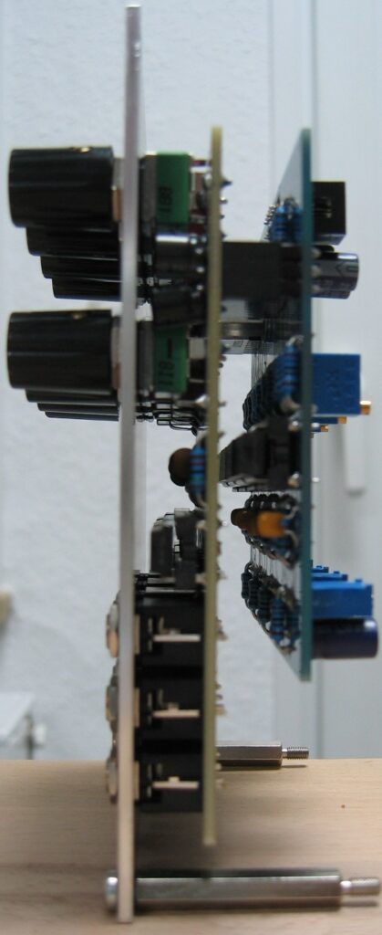
Modulation Sequencer front