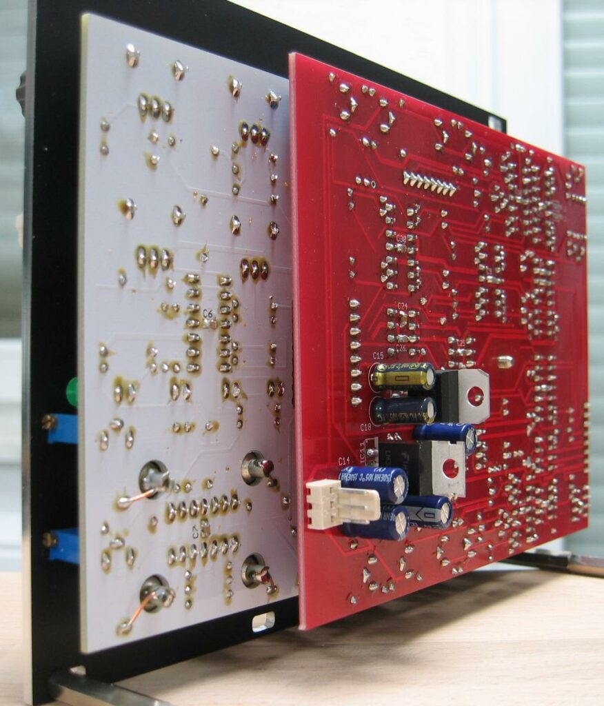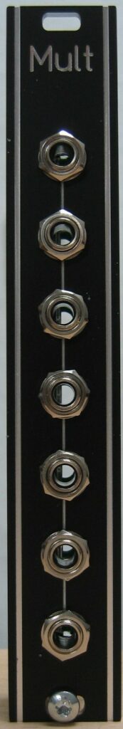
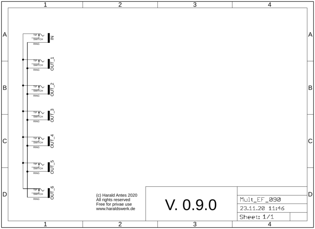
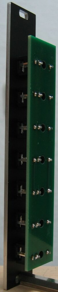
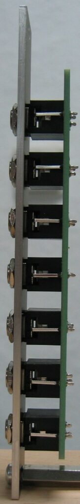
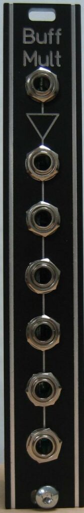
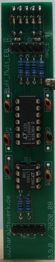
Just another often needed utility module. A passive multiple.
Specs and features
- Seven passive parallel in/outs
- No power connection
The documentation and the Gerber files for download can be found in my website.
Just another often needed utility module. A passive multiple.
The documentation and the Gerber files for download can be found in my website.
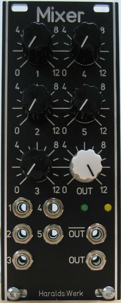
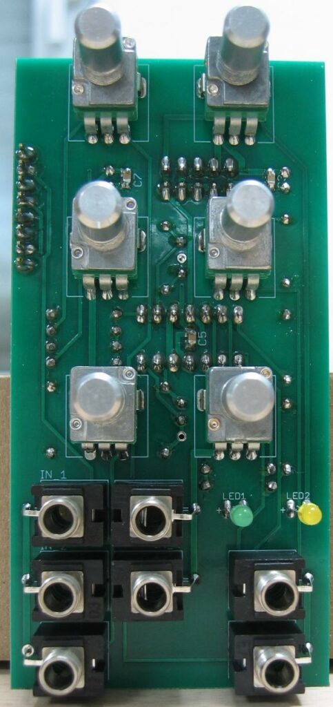
This is an often needed utility module. The mixer comes in handy for mixing CV sources and audio sources as well. This version is DC coupled, so you can use it for AC and DC mixing. There is an inverted output added. You can reverse the DC-CV mix with it or experiment with feedback loops in the audio domain. The added volume indicator us useful for finding the appropriate signal level. The volume indicator is optional. You can leave it out with no problems for the other functions.
The documentation and the Gerber files for download can be found in my website.
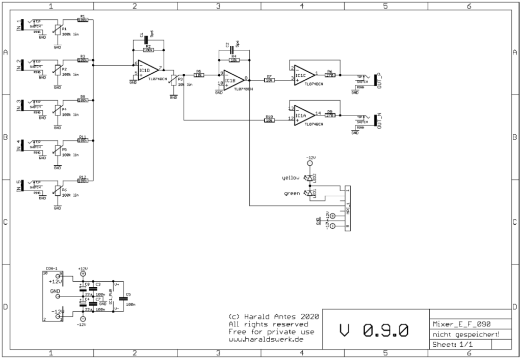
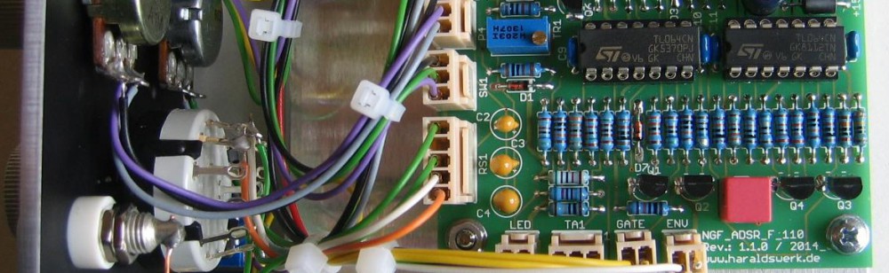
Control board: Straight forward design. The mixer is completely DC coupled. So you can use it for CV mixing as well as audio mixing. IC1D sums the five inputs and inverts the signal. P3 is used to adjust the overall signal level. IC1B inverts the signal again. IC1C and IC1A buffers the outputs.
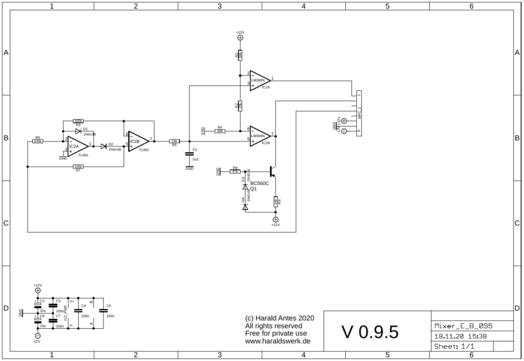
Level indicator: The circuitry around IC2 build an precision full wave rectifier. The output is smoothed with C1. The parts around the BC560C build a constant current source for driving the LED’s. The comparator LM393 (IC1A/B) switches the LED on and off according to the input level.
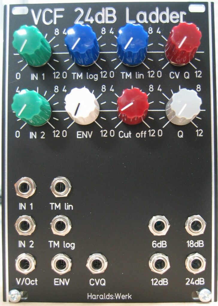
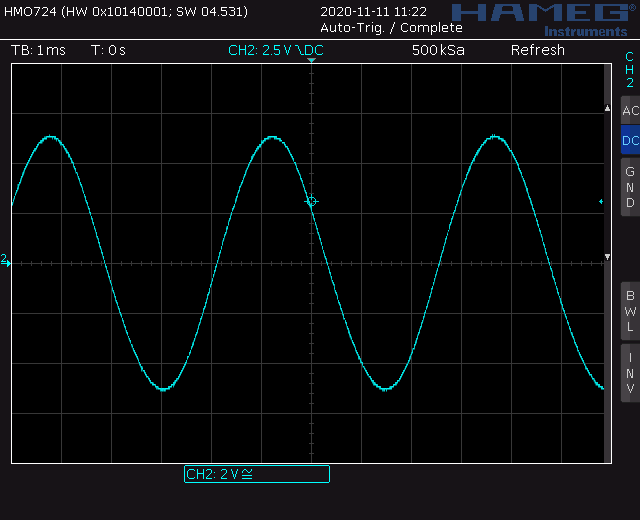
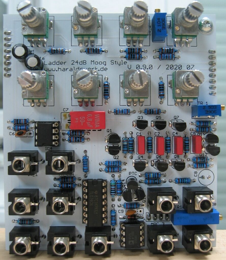
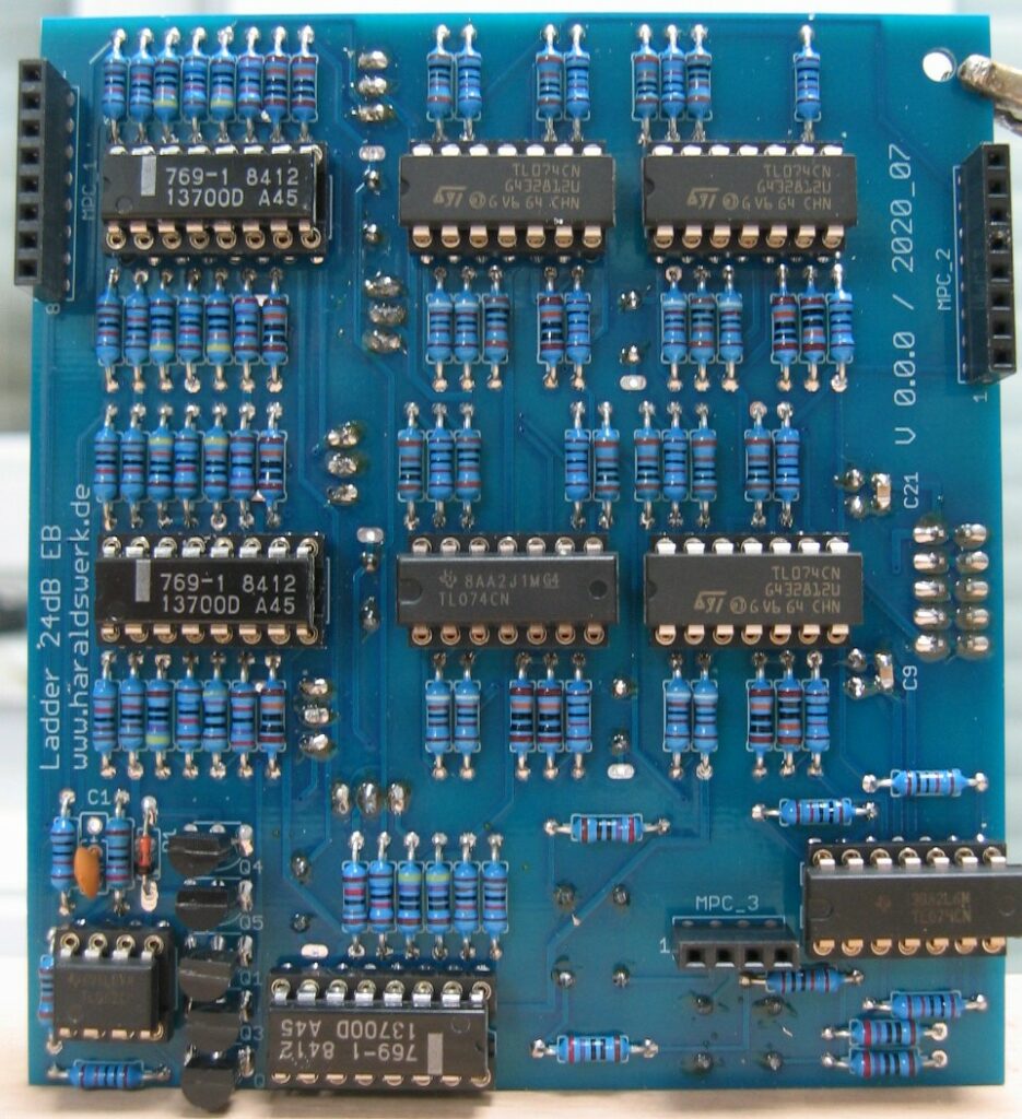
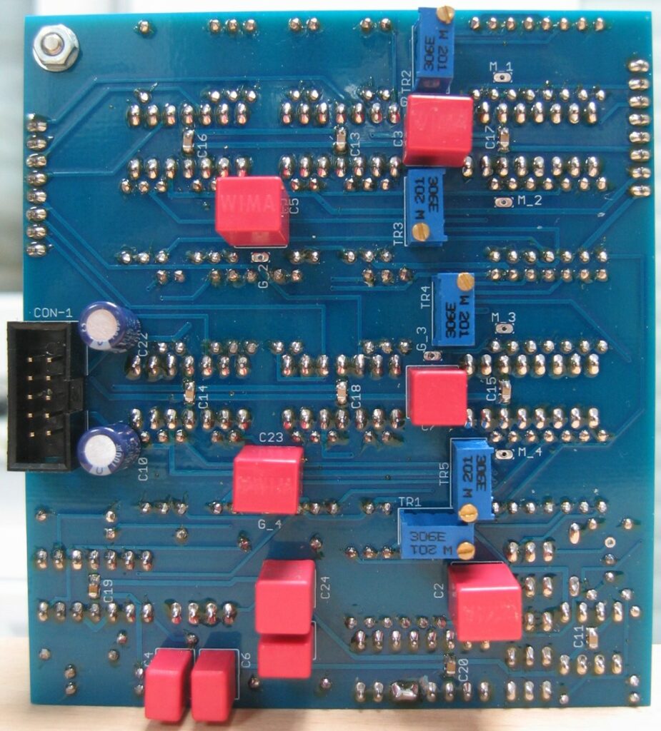
This is the Eurorack version of my NGF Moog Ladder Filter. I have brought out the 6dB, 12dB, 18dB and 24dB poles. Gain loss is corrected when turning up the emphasis/feedback. As a side effect off the gain corrections I got the emphasis voltage controlled as well. The exponential circuit is temperature compensated with KTY81-110. If the 12dB output is patched back to input 2 the filter can serve as a sine oscillator.
The documentation and the Gerber files for download can be found in my website.
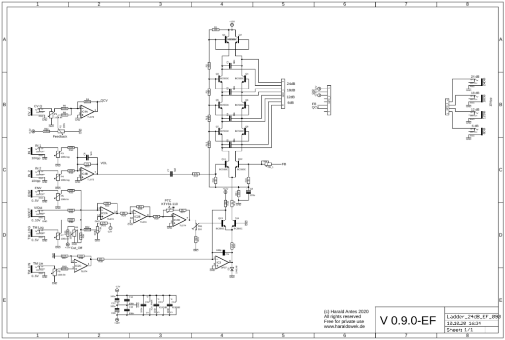
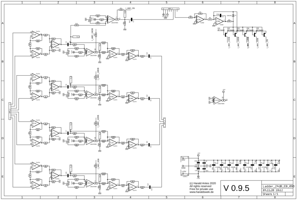
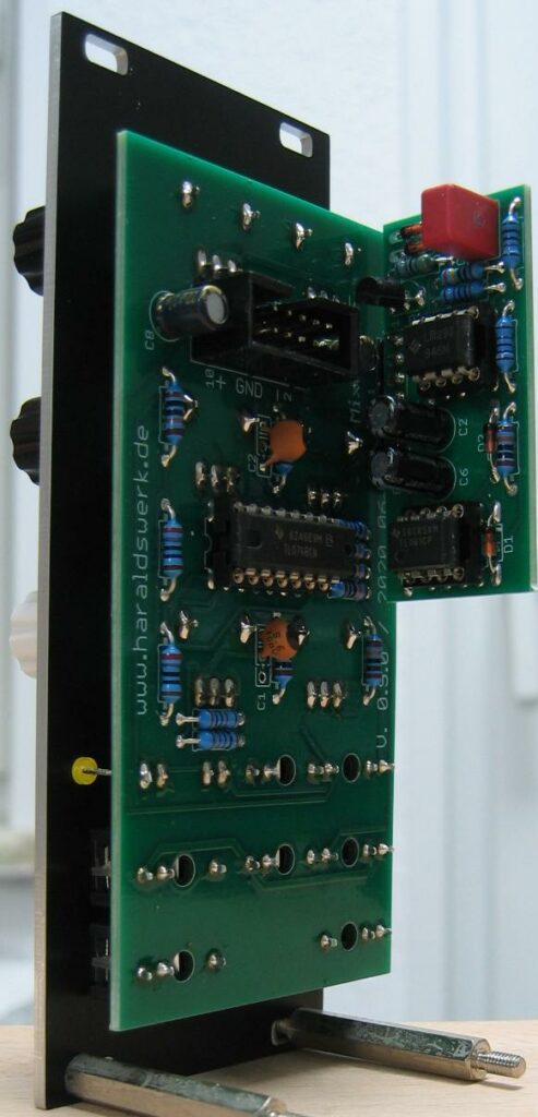
This is a classical Moog Ladder design implementation, nothing special to say about. All poles are brought out with instrumentation amplifiers. The voltage controlled emphasis is realized with means of one half LM13700 OTA (IC1OTA1). The control voltage for the emphasis is used to control the gain of four OTA (IC6OTA2, IC6OTA1, IC9OTA2, IC9OTA1) as well, one for each pole. The outputs of this OTA’s are added to the instrumentation amplifiers for each pole to compensate for the gain loss with high emphasis. The added amount is adjustable by changing one resistor (R28, R47, R66, R69). Higher values means higher gain. The temperature compensation for the expo-converter is realized with KTY81-110. This is not realy needed for a filter but a nice additional feature if you use the filter as sine VCO. If not wanted it is easily replaced with a 1k resistor.
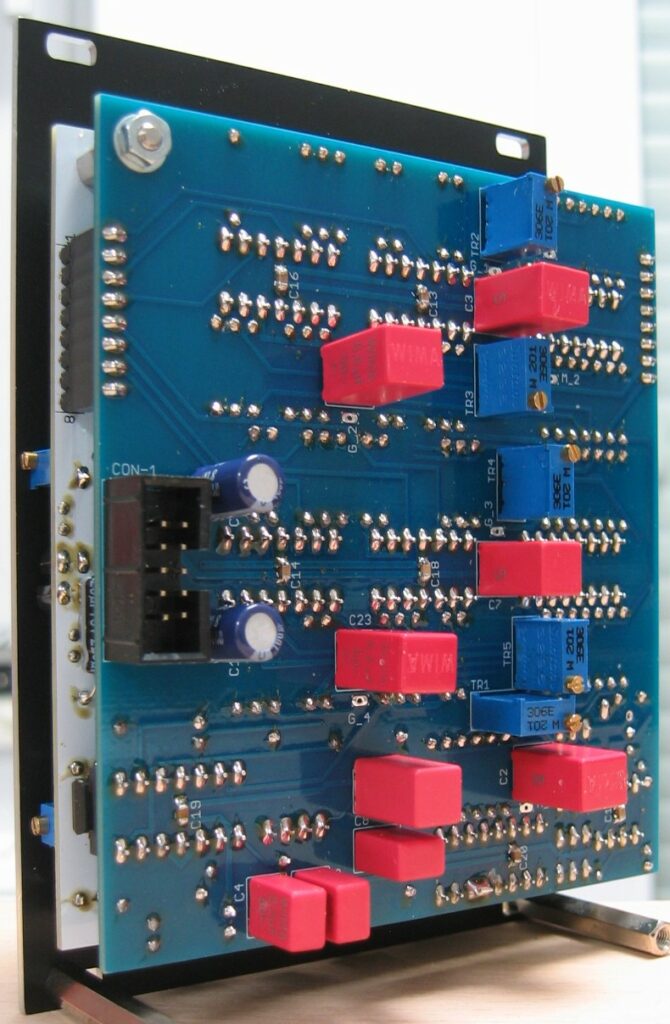
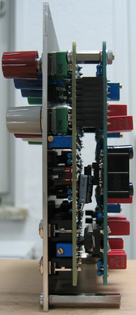
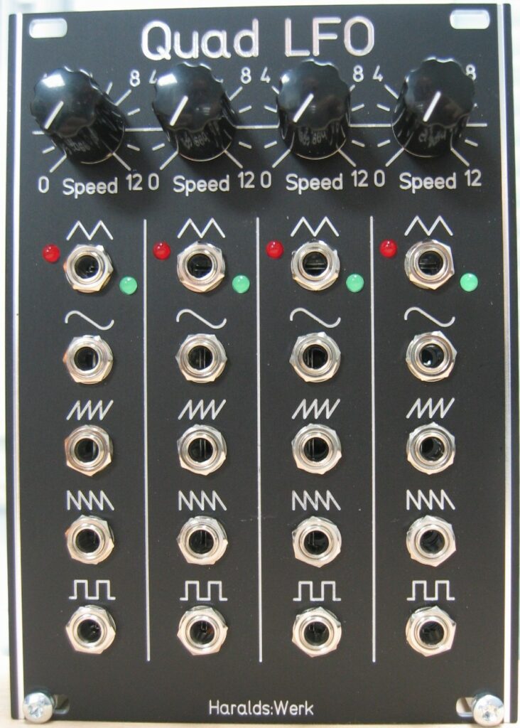
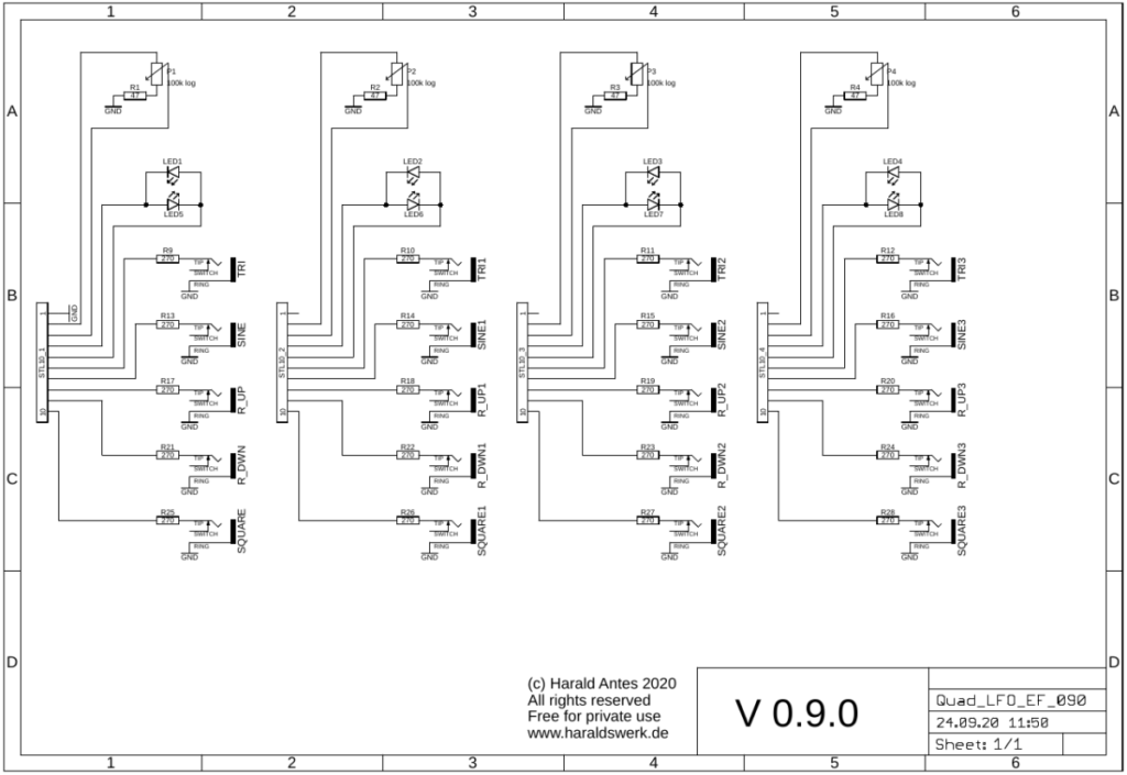
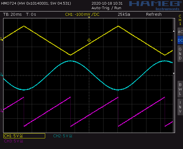
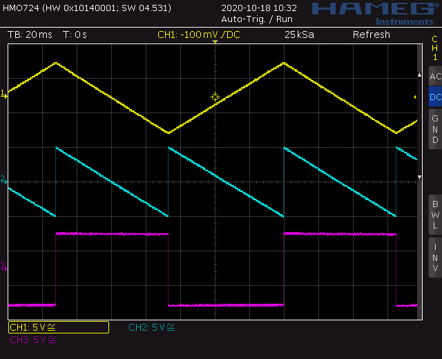
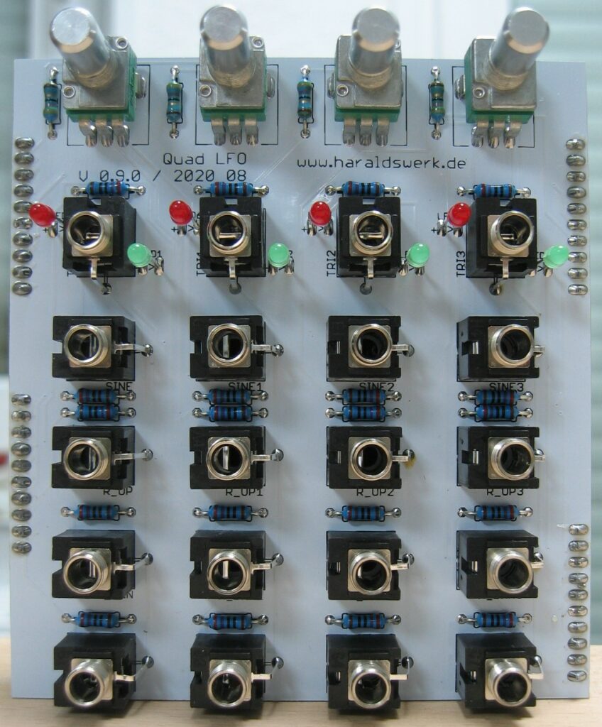
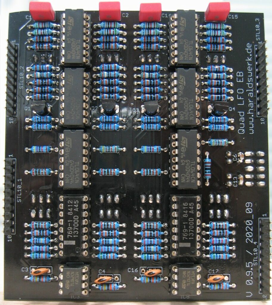
Four independent LFO with triangle, sine, ramp up, ramp down and square wave output. Output voltage 10Vpp. The sine is inverted against the triangle. Ramp up and ramp down are twice the frequency of the triangle.
Specs and features
The documentation and the Gerber files for download can be found in my website
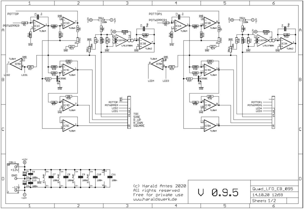
.Given for the first LFO. The oscillator consists of an integrator IC1C and an OpAmp Schmitt-Trigger IC1D. The triangle wave of the oscillator arises through the feedback of the trigger output to the input of the integrator. At the integrator output IC1C arises a triangle with the amplitude of the hysteresis of the Schmitt-Trigger. The input voltage of the integrator sets the rise and fall time of the voltage output. The square wave output is buffered with IC5C. The circuitry around IC4C provides the saw output. IC4D inverts the saw. The sine shaper is build with the OTA IC2OTA2 and IC3B. IC5D drives the LED.
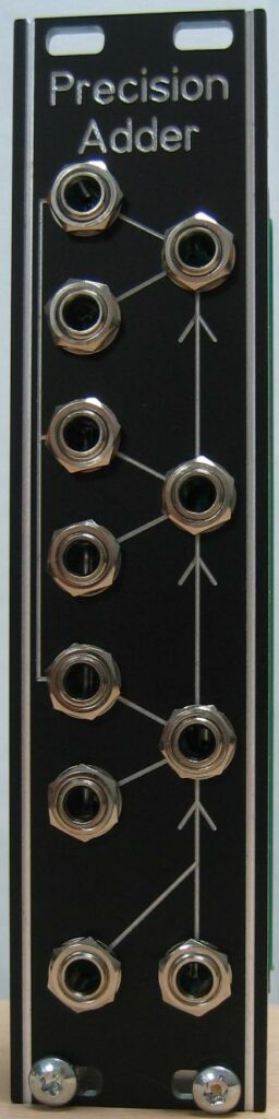
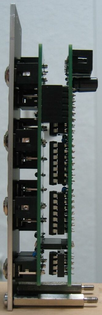
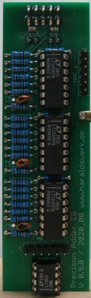
This is a useful and often needed utility module. The input voltages are precisely added to the outputs.The inputs 1, 3 and 5 are normalized. It can be used in different ways: As three independent adders, as buffered multiple, adding a modulation source simultaneously to all three outputs, adding two, three or four voltages precisely and a few more, depending on your patch. The accuracy depends on the used operational amplifier. For pitch CV I recommend precision OpAmps like the LT1014.
The documentation and the Gerber files for download can be found in my website.
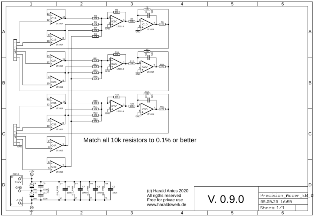
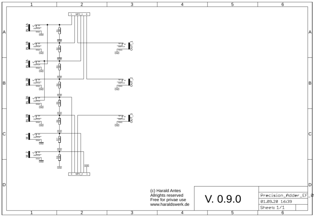
All inputs are buffered with high impedance inputs. They are followed by precision adders where the two inputs and the two additional modulation inputs are added together. The last stage buffers the output and corrects the phase. Inputs 1, 3 and 5 are normalized. The accuracy depends on the used operational amplifier and the matching of the resistors. For pitch CV I recommend precision OpAmps like the LT1014. Match all 10k resistors to 0,1% or better.
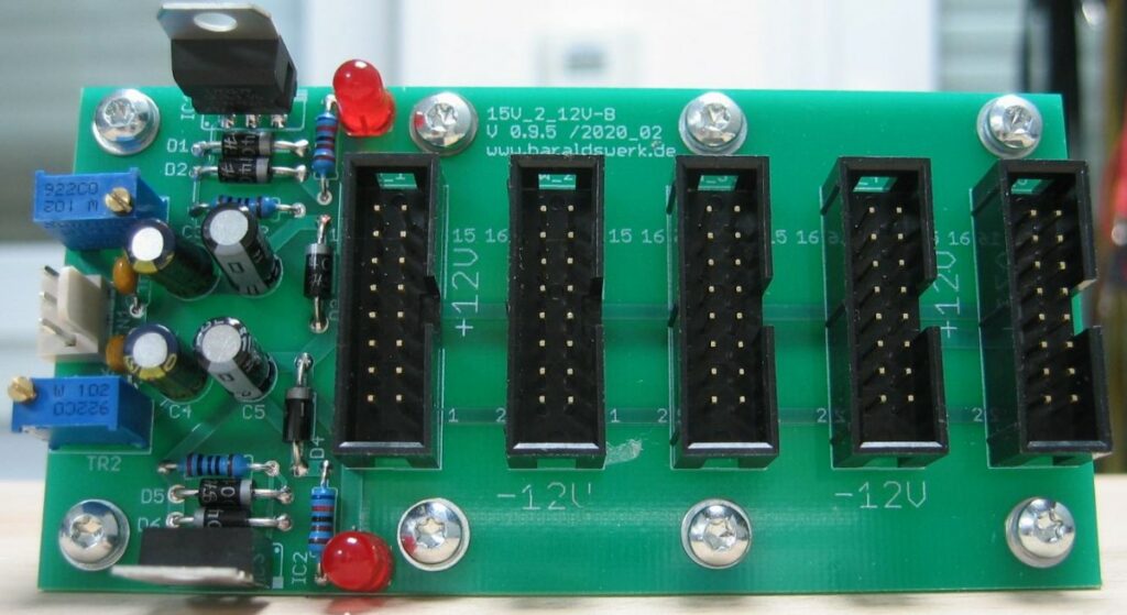
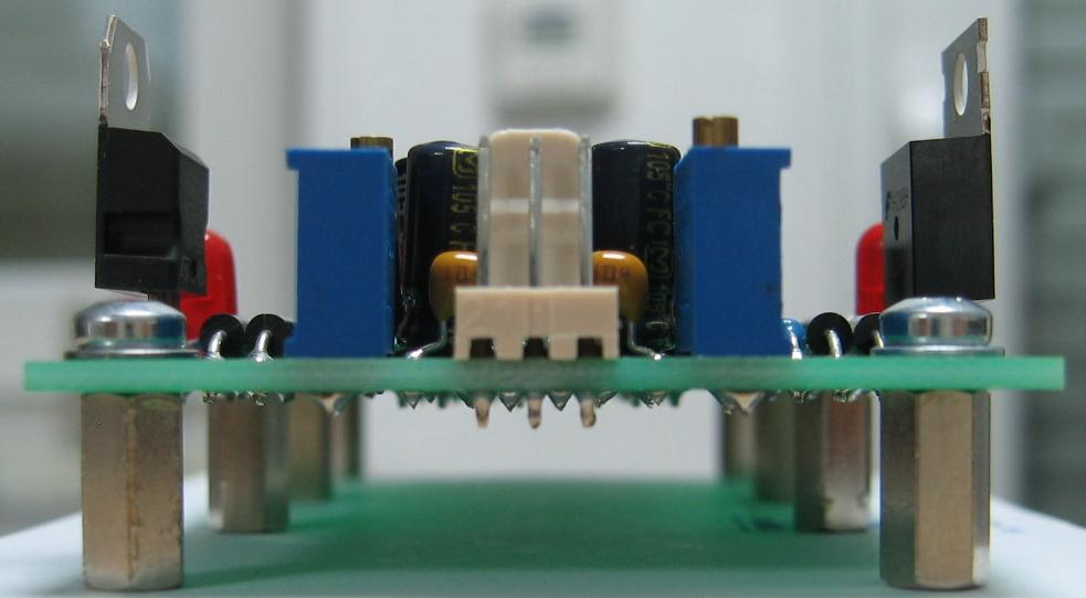
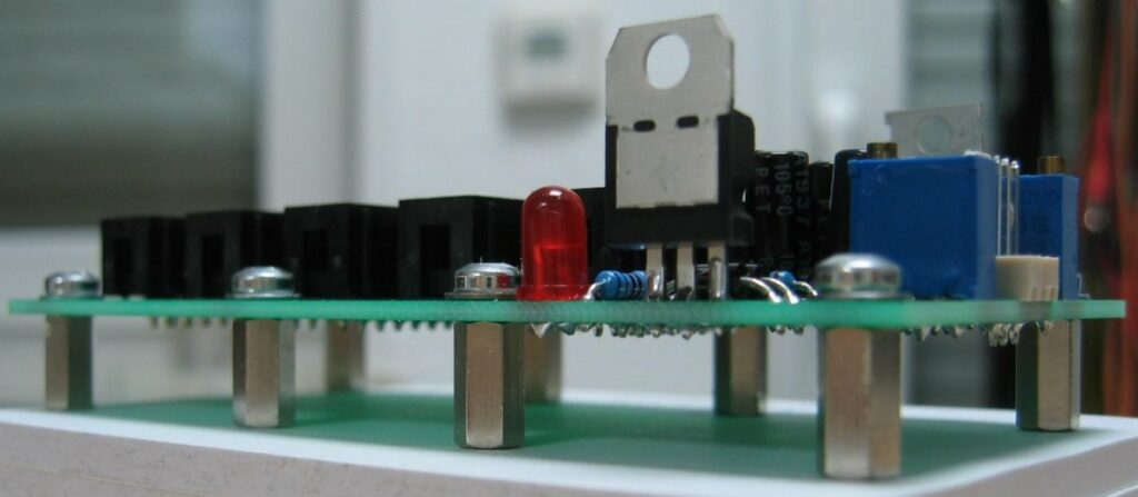
From time to time I want to integrate a 12V Eurorack module in my 15V banana setup. So I needed a 15V to 12V adaptor. Nothing spectacular. Just from the datasheet. This is the bigger brother for up to five modules from the single one.
The documentation and the Gerber files for download can be found in my website.
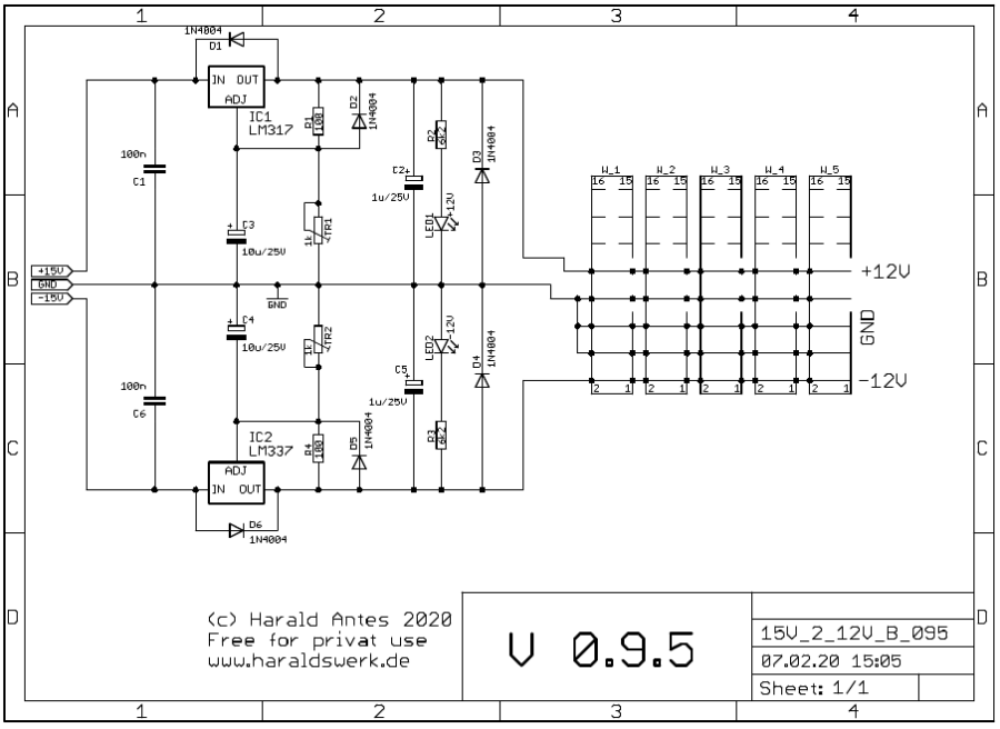
Just the standard configuration from the datasheets.
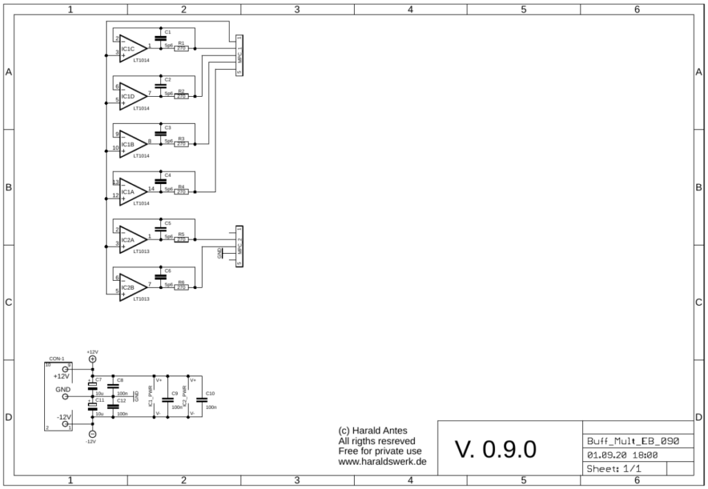
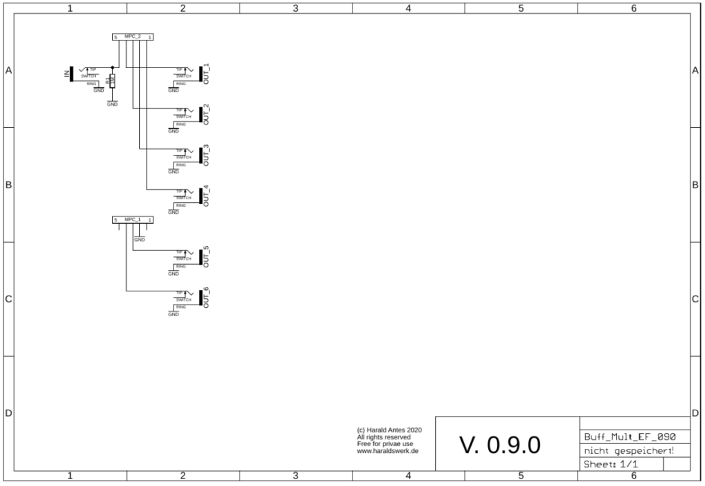
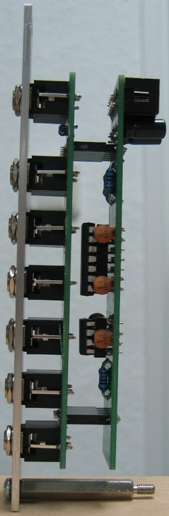
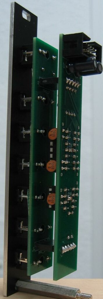
This is a useful and often needed utility module. The input voltage is precisely reproduced on the outputs. It comes in handy when you need to distribute signals which must be decoupled. The input signal is buffered and decoupled with means of individual operational amplifiers. One input drives 6 individual outputs. The accuracy depends on the used operational amplifier. For pitch CV I recommend precision OpAmps like the LT1014 (quad) and LT1013 (dual).
The documentation and the Gerber files for download can be found in my website.
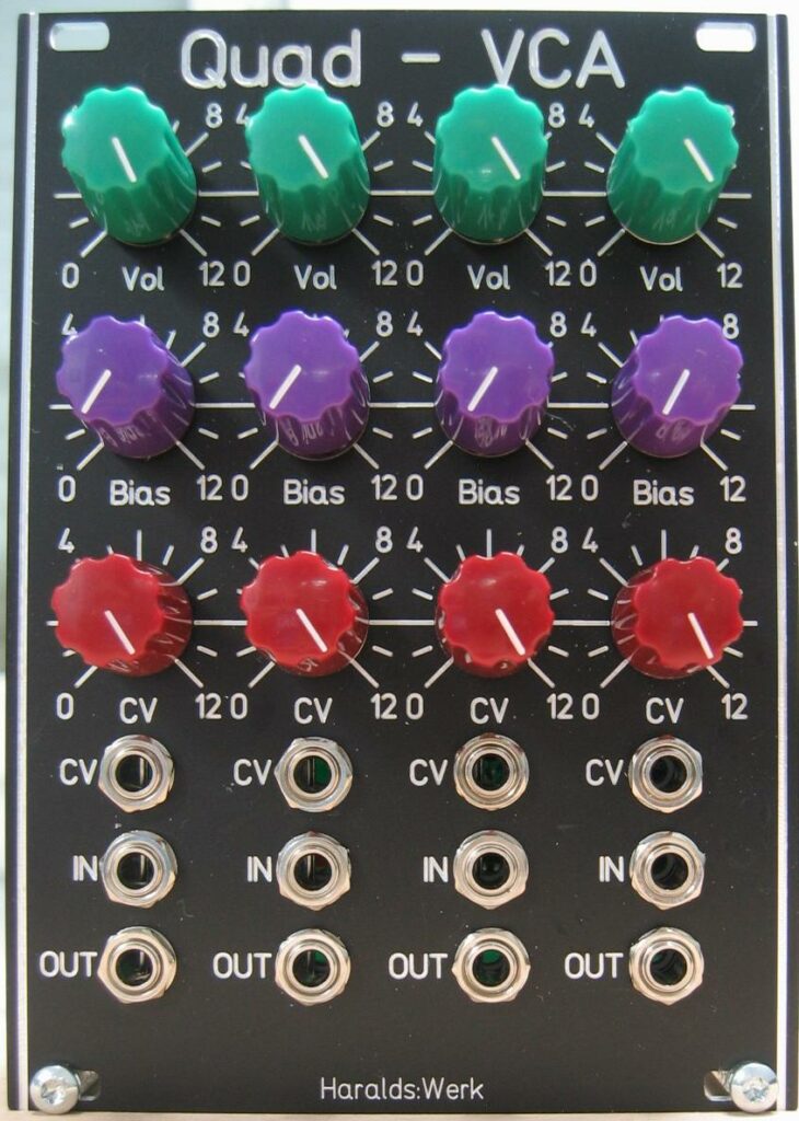
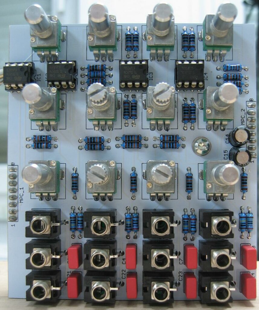
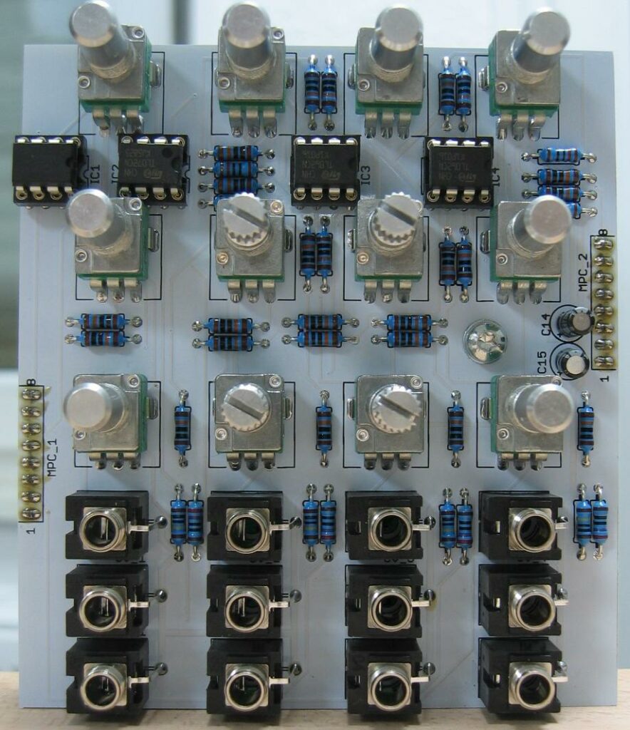
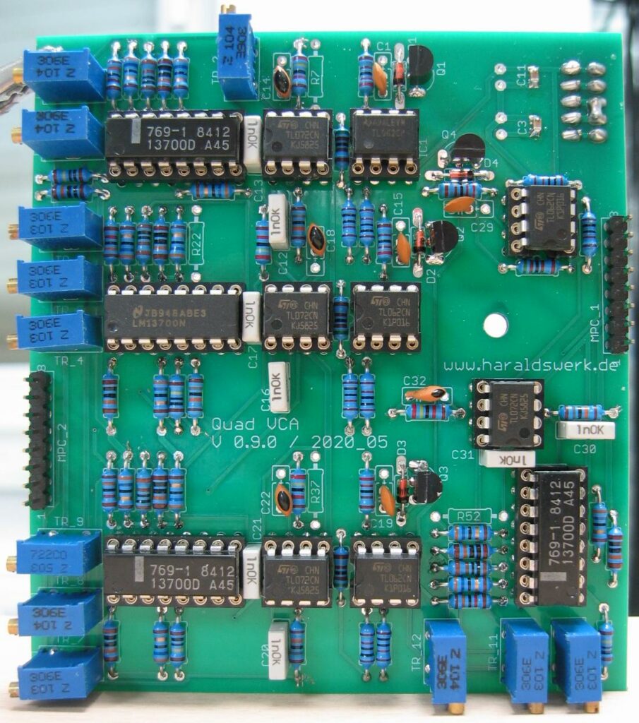
This is one more module for my quad system. It contains four VCA with normalized input, so you can distribute one input signal to four output channels. With each channel under voltage control you can move the input signal through the room dependent on the control voltages. I have two versions build one AC and the other DC coupled. Beside using this VCA’s for signal distribution you can use every VCA independently. The gain to voltage ratio is linear. This is done because it is easier to predict the performance. The distribution of the signal must be steered through the control voltages. The implementation follows the recommendations from an article at Open Music Labs from October 3, 2015 (Minimizing distortion in OTA’s)
The documentation and the Gerber files for download can be found in my website.
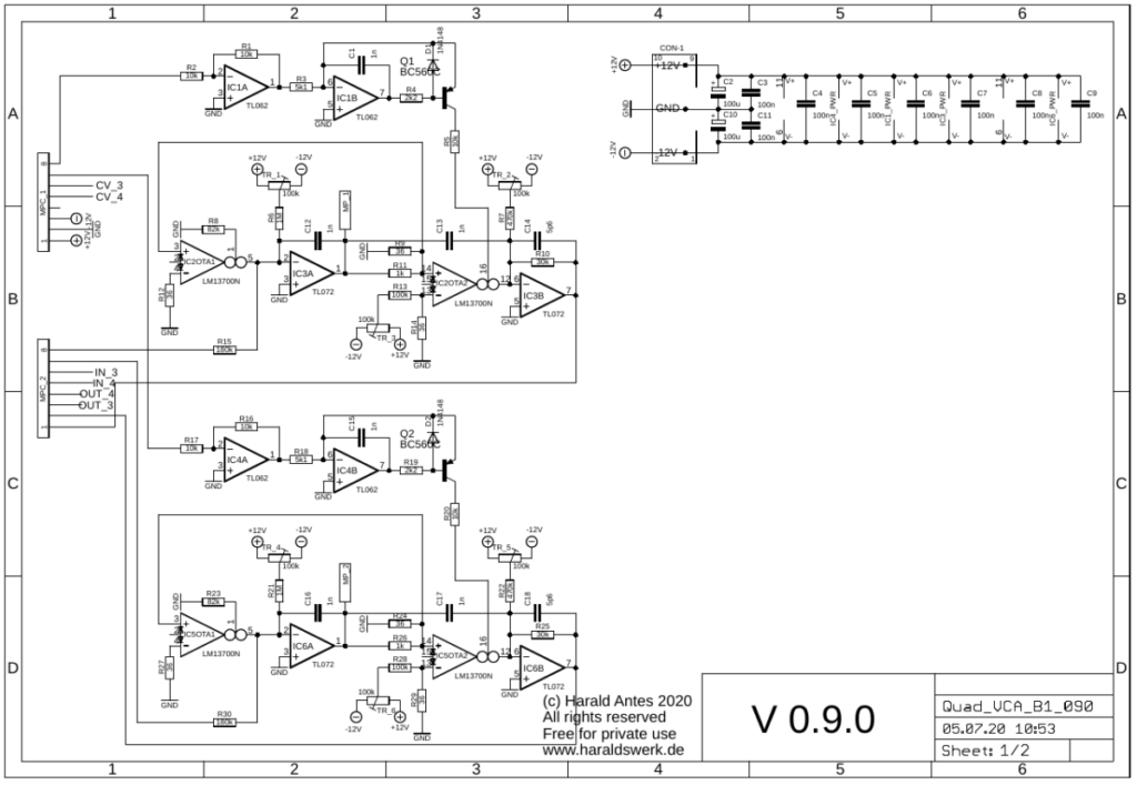
The linear controlled current source for Iabc is straight forward and implemented as usual. An elaborate description for the VCA part is given here.
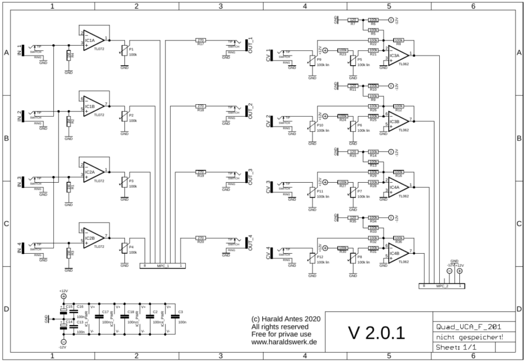
On the left side are the potentiometers for volume control followed by the input buffers. The only difference between AC and DC coupling are the capacitors. On the right side are the CV input potentiometers and the bias potentiometers followed by the voltage adder.
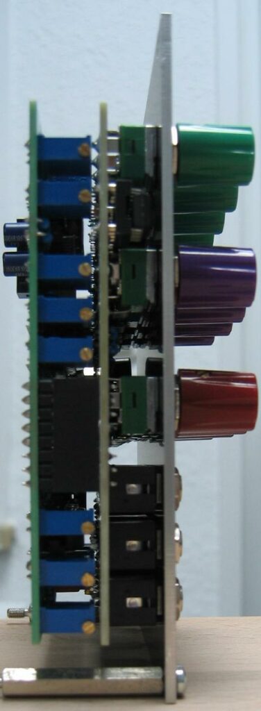
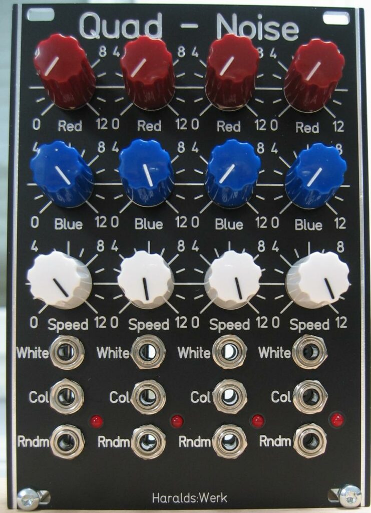
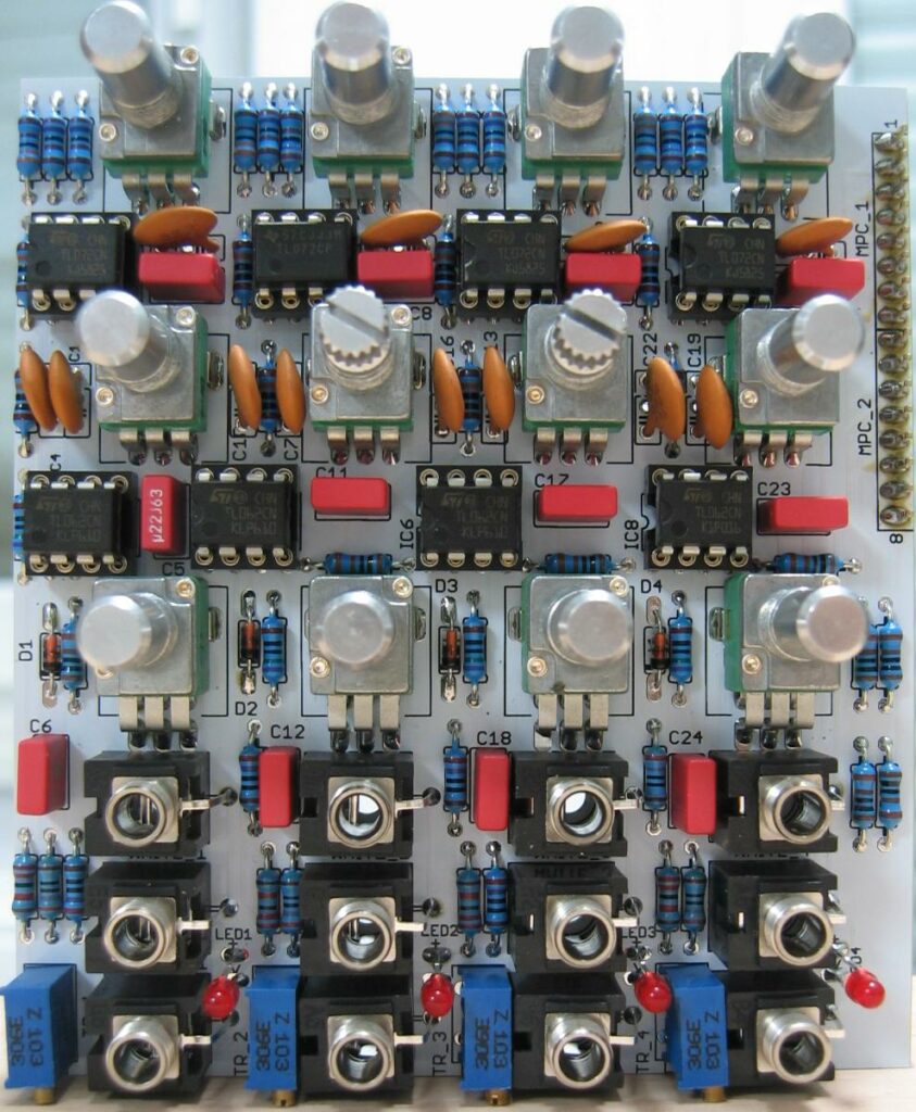
It is quite useful to have different adjustable noise and random voltage sources. Depending on your patch stile of course. Here is the quad version of my noise module from the NGF project. It is a combination of two original Elektor Formant modules. The noise module from Elektor Formant book one and the colored noise (CNC) module from book two. It provides four independent white noise outputs, four adjustable colored noise outputs with “red” and “blue” adjustment. The four random voltage outputs are adjustable in speed of change. The noise is derived from the reverse biased BE diode of an NPN transistor.
The documentation and the Gerber files for download can be found in my website.
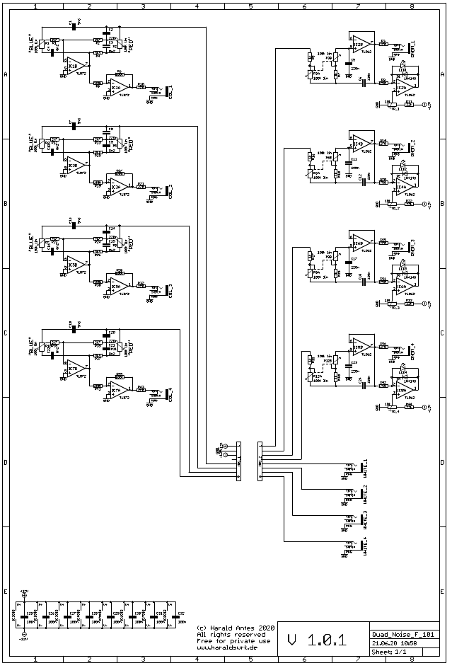
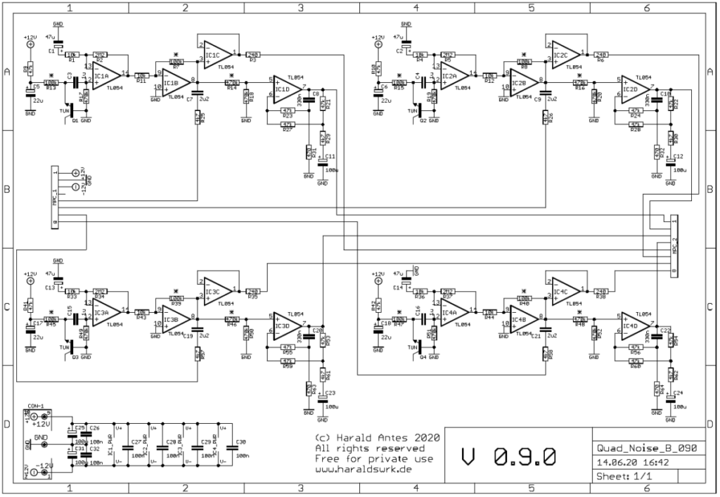
(Given for one of the four.) Noise source is the reverse biased BE diode of NPN transistor Q1 (B_090). The following operational amplifier IC1A and IC1B (B_090) amplifies the noise to 10Vpp. IC1C (B_090) is the buffer for the white noise output. IC2B (F_101) is configured as a 12dB low pass. So you get a low frequency random voltage. The changing speed is set with P3A/P3B (F_101) which sets the corner frequency of the low pass filter. IC2A / LED1 (F_101) makes the fluctuation visible. TR_1 (F_101) adjust the brightness of LED1 (F_101). In the feedback loop of IC1B (F_101) is an adjustable filter combination which gives you a wide range of adjustable colored noise with P1 and P2 (F_101). The output is buffered with IC1A (F_101).
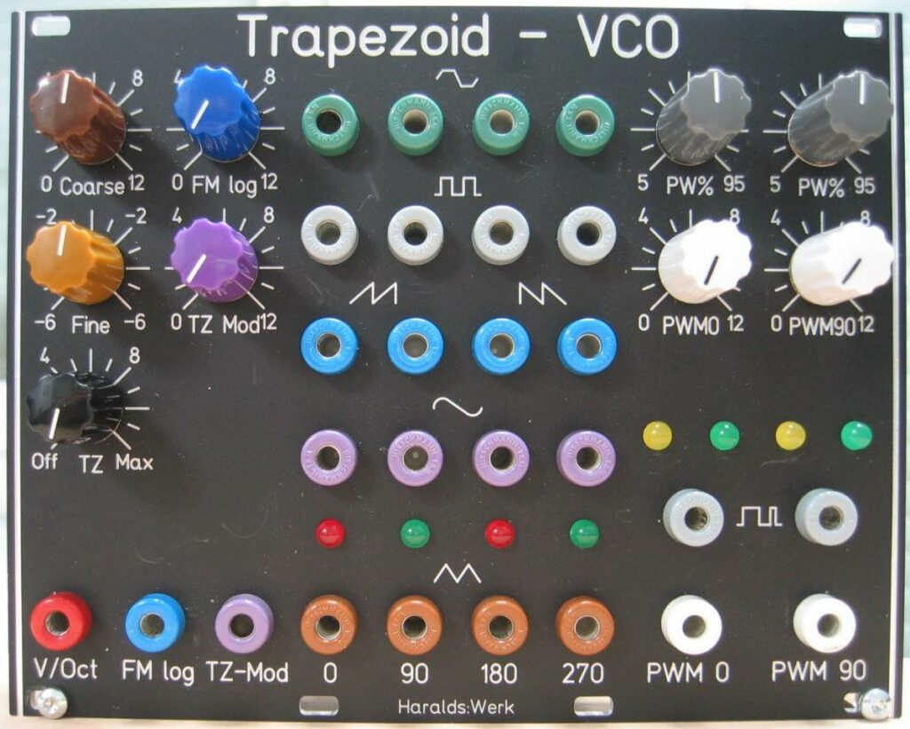
This is my second take on the Trapezoid VCO designed by Don Tillman. My first implementation can be found here. This time I mounted the PCB’s parallel to the front to save space and integrated the wave shapers. The core is still based on the original design from Don (used with permission). I found the original article and schematic about the Trapezoid VCO on Don Tillman’s site (Link to original article from 19 July 2003). The article consists off three parts with the core implementation in part 2. I kept the basic idea and changed nearly everything else. I use an other exponentiator scheme and temperature stabilization. Another reference voltage device is used. And quadrature square outputs are implemented. As well as the additional waveforms triangle, sine, ramp up, ramp down and pulse.
The documentation and the Gerber files for download can be found in my website.